Complementary barrier superlattice long-wave infrared detector

A long-wave infrared and superlattice technology, applied in semiconductor devices, electrical components, circuits, etc., can solve the problems of not being able to receive normal incident light, increase process complexity, and low quantum efficiency, so as to reduce G-R dark current, The effect of reducing tunneling dark current and high detection rate

Pending Publication Date: 2021-06-25
INST OF SEMICONDUCTORS - CHINESE ACAD OF SCI
View PDF4 Cites 3 Cited by
  • Summary
  • Abstract
  • Description
  • Claims
  • Application Information

AI Technical Summary

Problems solved by technology

[0003] However, HgCdTe materials have poor uniformity in a large area in the long-wave band, and the yield rate is low; QWIP uses transitions between subbands, so the quantum efficiency is low, and according to the transition selection rule, it cannot receive normal incident light, so gratings need to be fabricated on the surface, which increases the process complexity

Method used


Image

  • Complementary barrier superlattice long-wave infrared detector
  • Complementary barrier superlattice long-wave infrared detector
  • Complementary barrier superlattice long-wave infrared detector

Examples


Embodiment

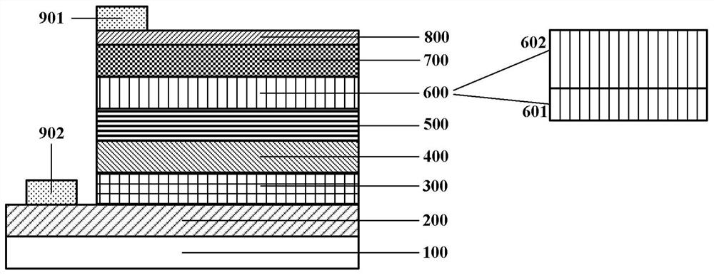
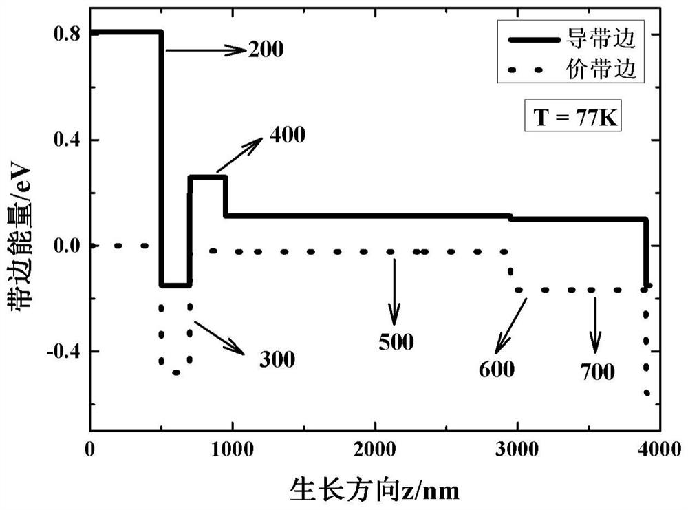
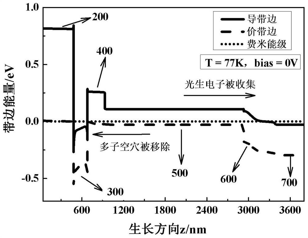
[0047]A layer of gradedly doped P-type GaSb buffer layer 200 is grown on the P-type GaSb substrate 100 by using molecular beam epitaxy equipment as a bottom contact layer. Then, an n-type gradually doped n-type InAsSb layer 300 is grown on the p-type GaSb buffer layer 200 to remove excess holes in the absorption region. An electron barrier layer 400 of InAs / GaSb superlattice material is grown on the n-type InAsSb layer 300 to block reverse injection electrons of the n-type InAsSb layer 300 . Next, the absorption region 500 of the InAs / GaSb superlattice material is grown on the electron barrier layer, and the InAs / GaSb / AlSb / GaSb superlattice material composed of InAs / GaSb / AlSb / GaSb superlattice material gradually doped from P to N from bottom to top The hole barrier layer 600 , further, the hole barrier layer 600 includes from bottom to top: a p-type doped hole barrier region 601 and an n-type doped hole barrier region 602 . Gradual n-type doped n-type contact layer 700 is gro...


PUM

PropertyMeasurementUnit
thicknessaaaaaaaaaa
thicknessaaaaaaaaaa
thicknessaaaaaaaaaa

Abstract

The invention provides a complementary barrier superlattice long-wave infrared detector, which sequentially comprises a substrate, a buffer layer, an n-type InAsSb layer, an electron barrier layer, an absorption layer, a hole barrier layer, an n-type contact layer and a cover layer from bottom to top, wherein the hole barrier layer comprises a p-type doped hole barrier region and an n-type doped hole barrier region from bottom to top, the complementary barrier superlattice long-wave infrared detector further comprises an upper electrode and a lower electrode, the upper electrode is arranged on the cover layer, and the lower electrode is disposed on the buffer layer. According to the invention, the G-R current of the long-wave detector can be suppressed, and the turn-on voltage of the device is reduced.

Description

technical field [0001] The disclosure relates to the field of semiconductor chip manufacturing, in particular to a complementary barrier superlattice long-wave infrared detector. Background technique [0002] Currently, the mainstream long-wavelength detector materials include mercury cadmium telluride, quantum well (QWIP) and InAs / GaSb superlattice. [0003] However, HgCdTe materials have poor uniformity in a large area in the long-wave band, and the yield rate is low; QWIP uses transitions between subbands, so the quantum efficiency is low, and according to the transition selection rule, it cannot receive normal incident light, so gratings need to be fabricated on the surface, which increases the The complexity of the process. [0004] Therefore, InAs / GaSb superlattice has become the most eye-catching third-generation detector material. InAs / GaSb superlattice bandgap can be adjusted flexibly by changing superlattice components, and has the advantages of large electronic ...

Claims


Application Information

Patent Timeline
Patent Type & Authority Applications(China)
IPC IPC(8): H01L31/109H01L31/0304H01L31/0352
CPCH01L31/109H01L31/03046H01L31/035236
Inventor 崔素宁蒋洞微李勇陈伟强蒋俊锴王国伟徐应强牛智川
Owner INST OF SEMICONDUCTORS - CHINESE ACAD OF SCI
Why Eureka
Try Eureka