Sampling hold circuit structure for realizing offset elimination function

A sample-and-hold circuit and circuit structure technology, applied in the direction of physical parameter compensation/prevention, etc., can solve the problems of analog-to-digital converter precision decline, large v0, difficult control of Vos1, etc., to eliminate offset voltage errors, reduce difficulty, and ensure The effect of precision

Pending Publication Date: 2021-07-09
CRM ICBG (WUXI) CO LTD
View PDF0 Cites 0 Cited by
  • Summary
  • Abstract
  • Description
  • Claims
  • Application Information

AI Technical Summary

Problems solved by technology

Among them, Vos1 is related to the gain of the operational amplifier AMP1. The larger the gain, the smaller the Vos1, but the more complex the structure of AMP1 will be designed, the higher the cost. At the same time, because Vos1 is also related to the matching of the device in the process of manufacturing, so Vos1 is a random quantity that is difficult to control
The error v0 introduced by the channel charge injection and clock feedthrough effect is related to the size of the CMOS switch, and usually want to fast sampling speed, will choose larger size P1 and N1 transistors, which will lead to larger v0
The above shortcomings will directly lead to a decrease in the accuracy of the entire analog-to-digital converter

Method used


Image

  • Sampling hold circuit structure for realizing offset elimination function
  • Sampling hold circuit structure for realizing offset elimination function
  • Sampling hold circuit structure for realizing offset elimination function

Examples


Embodiment Construction

[0018] In order to describe the technical content of the present invention more clearly, further description will be given below in conjunction with specific embodiments.

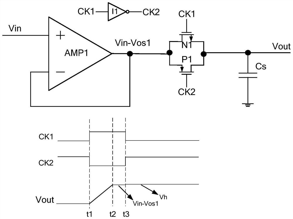
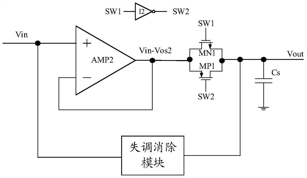
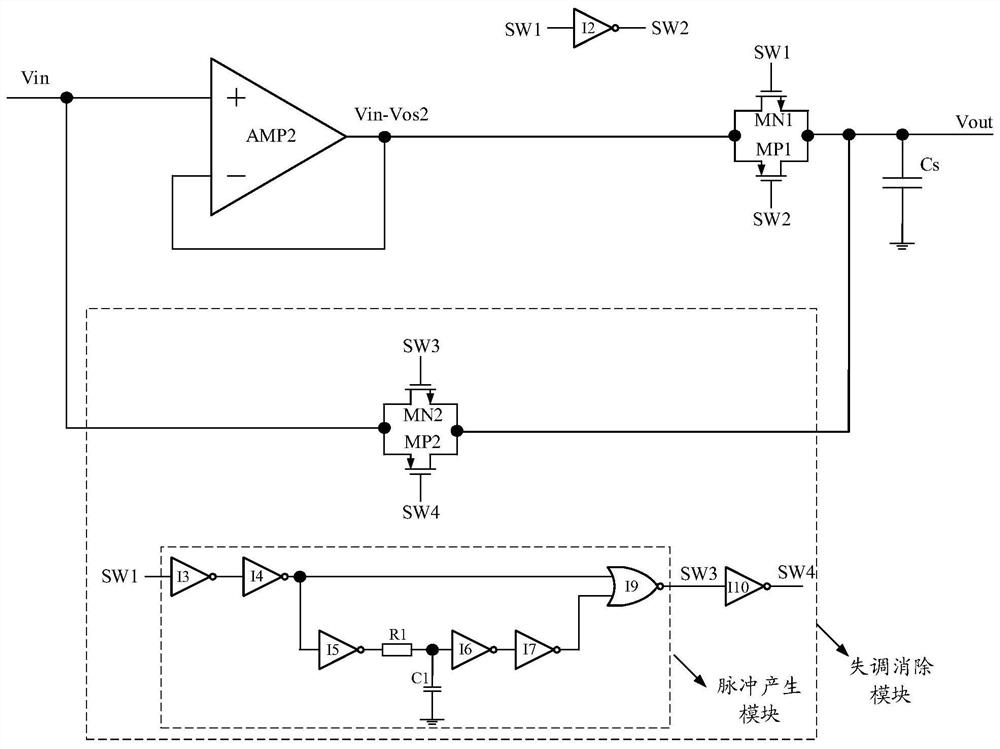
[0019] The sample-and-hold circuit structure of the present invention that realizes the offset elimination function includes an operational amplifier, a first CMOS transmission gate module, and an offset elimination module. The positive input terminal of the operational amplifier is connected to the input signal, and the output terminal is connected to the first CMOS transmission gate module. The gate module is connected, and the negative input terminal of the operational amplifier is connected with the output terminal as a unity gain buffer, and the two ends of the offset elimination module are respectively connected to the positive input terminal of the operational amplifier and the output terminal of the CMOS transmission gate module. connected, the offset elimination module is used to eliminate the influ...


PUM


Abstract

The invention relates to a sampling hold circuit structure for realizing a detuning elimination function, which comprises an operational amplifier, a first CMOS (Complementary Metal Oxide Semiconductor) transmission gate module and a detuning elimination module, the positive input end of the operational amplifier is connected with an input signal, and the output end of the operational amplifier is connected with the first CMOS transmission gate module; the negative input end of the operational amplifier is connected with the output end of the operational amplifier to serve as a unit gain buffer, the two ends of the offset elimination module are connected with the positive input end of the operational amplifier and the output end of the CMOS transmission gate module respectively, and the offset elimination module is used for eliminating the influence of offset voltage introduced by the operational amplifier. By adopting the sampling hold circuit structure for realizing the offset elimination function, the offset voltage error of the operational amplifier is eliminated, the design difficulty of the operational amplifier is reduced, and meanwhile, the cost is reduced. The large-size MP1 and MN1 and the minimum-size MP2 and MN2 are adopted, the high sampling speed is met, and meanwhile the precision of the whole analog-to-digital converter is guaranteed.

Description

technical field [0001] The invention relates to the field of integrated circuits, in particular to the field of sample-and-hold circuits, in particular to a sample-and-hold circuit structure for realizing the function of eliminating offset. Background technique [0002] The circuit structure of the prior art such as figure 1 As shown, the input signal Vin is connected to the positive input terminal of the operational amplifier AMP1, and AMP1 is connected in the form of a unity gain buffer, and the output terminal of AMP1 is connected to the sampling capacitor Cs through the CMOS transmission gate composed of PMOS transistor P1 and NMOS transistor N1. CK1 and CK2 respectively control the gates of N1 and P1, CK1 and CK2 are in an inverse relationship, and CK1 generates CK2 through inverter I1. [0003] Due to the offset voltage of the operational amplifier AMP1, the output voltage of AMP1 is Vin-Vos1, where Vos1 is the offset voltage of AMP1, and the voltage value depends on ...

Claims


Application Information

Patent Timeline
Patent Type & Authority Applications(China)
IPC IPC(8): H03M1/06
CPCH03M1/06
Inventor 曾洁琼张天舜刘玉芳丁增伟
Owner CRM ICBG (WUXI) CO LTD
Why Eureka
Try Eureka