Check patentability & draft patents in minutes with Patsnap Eureka AI!

Semiconductor device and crack detection method

A crack detection and semiconductor technology, which is applied in semiconductor devices, semiconductor/solid-state device testing/measurement, semiconductor/solid-state device components, etc., can solve problems such as undetectable cracks and achieve high-precision detection effects

Pending Publication Date: 2021-07-20
MITSUBISHI ELECTRIC CORP
View PDF1 Cites 0 Cited by
  • Summary
  • Abstract
  • Description
  • Claims
  • Application Information

AI Technical Summary

Problems solved by technology

[0006] In the technique of Patent Document 1, since the presence or absence of a crack is determined based on the resistance value of the crack detection wiring (diffusion layer or electrode), if the crack does not change significantly to the extent that the resistance value of the crack detection wiring greatly changes cut into the wiring, the crack cannot be detected
Therefore, the technology of Patent Document 1 is difficult to detect the development of cracks with high precision.

Method used


Image

  • Semiconductor device and crack detection method
  • Semiconductor device and crack detection method
  • Semiconductor device and crack detection method

Examples


Embodiment approach 1

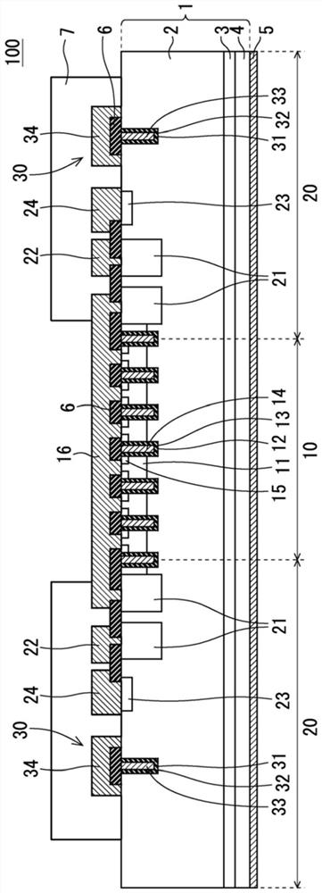
[0021] figure 1 It is a cross-sectional view showing the structure of the semiconductor device 100 according to the first embodiment. In the present embodiment, the semiconductor element included in the semiconductor device 100 is an insulated gate type, more specifically, a trench gate type IGBT (Insulated Gate Bipolar Transistor). However, the semiconductor element may be, for example, elements other than IGBTs such as MOSFETs (Metal-Oxide-Semiconductor Field Effect Transistors) and diodes. In addition, the IGBT and MOSFET may be of planar gate type. In addition, in the following description, the first conductivity type is referred to as N type, and the second conductivity type is referred to as P type, but it is also possible to reverse this, and the first conductivity type is referred to as P type, and the second conductivity type is referred to as N type. type.

[0022] The semiconductor device 100 is formed using a semiconductor substrate 1 as a semiconductor layer. ...

Embodiment approach 2

[0041] Figure 4 It is a cross-sectional view showing the structure of the semiconductor device 100 according to the second embodiment. Figure 4 The right half of the cross section of the semiconductor device 100 is enlarged in the middle. In addition, in Figure 4 in, right with figure 1 Components that are the same as those shown are assigned the same reference numerals, and therefore descriptions thereof will be omitted here.

[0042] In the semiconductor device 100 according to Embodiment 2, the additional inner wall insulating film 32 a made of, for example, a silicon oxide film is stacked on the inner wall insulating film 32 of the crack detection structure 30 . Therefore, the actual thickness of the inner wall insulating film 32 (including the thickness of the additional inner wall insulating film 32 a ) is larger than the thickness of the gate insulating film 13 . In the following description of Embodiment 2, "the thickness of the inner wall insulating film 32" me...

Embodiment approach 3

[0046] Figure 5 is a cross-sectional view showing the structure of the semiconductor device 100 according to the third embodiment. exist Figure 5 In , the right half of the cross section of the semiconductor device 100 is also enlarged and shown. In addition, in Figure 5 in, right with figure 1 Components that are the same as those shown are assigned the same reference numerals, and therefore descriptions thereof will be omitted here.

[0047] In the semiconductor device 100 according to Embodiment 3, the trench 31 of the crack detection structure 30 is formed in the N-type drift layer 2 , but the second conductivity type is formed in the vicinity of the trench 31 to cover the periphery of the trench 31 . The P-type region 36. By forming the PN junction formed by the N-type drift layer 2 and the P-type region 36 around the trench 31, it is possible to reduce the voltage applied to the inner wall insulating film 32 when a voltage is applied between the collector electro...


PUM


Abstract

The invention relates to a semiconductor device and a crack detection method. Provided is a semiconductor device that can detect the cracking progress with high precision. The semiconductor device 100 is formed using a semiconductor substrate 1, and includes an active region 10 in which a semiconductor element is formed, and an edge termination region 20 outside the active region 10. A crack detection structure 30 is termed in the edge termination region 20 of the semiconductor substrate 1. The crack detection structure 30 includes: a trench 31 formed in the semiconductor substrate 1 and extending in a circumferential direction of the edge termination region 20; an inner-wall insulating film 32 formed on an inner wall of the trench 31; an embedded electrode 33 formed on the inner-wall insulating film 32 and embedded into the trench 31; and a monitor electrode 34 formed on the semiconductor substrate 1 and connected to the embedded electrode 33.

Description

technical field [0001] The present invention relates to semiconductor devices, and more particularly to techniques for detecting cracks generated in semiconductor devices. Background technique [0002] In response to market demands for energy saving and miniaturization of power devices, wafer thinning for the purpose of reducing losses in actual use of power devices is being promoted. If the wafer is made thinner, electrical characteristics are improved, but there are problems in mass productivity such as difficulty in handling the wafer and restrictions on various processes involved in the manufacture of semiconductor devices. In particular, in the dicing process of cutting out individual chips from the wafer, since the wafer is physically cut by a diamond cutter or the like, foreign matter on the wafer, chipping of the cutter, warpage of the wafer, surface condition of the wafer, etc. Cracks, chips, etc. (hereinafter collectively referred to as "cracks") occur at the dici...

Claims


Application Information

Patent Timeline
IPC IPC(8): H01L23/544H01L21/66G01N27/00
CPCH01L23/544H01L22/34H01L22/32H01L22/12H01L22/14G01N27/00G01R31/2858G01R31/2884G01R31/2644H01L29/7802H01L29/7813H01L29/7811H01L29/7397H01L29/0615H01L29/0619H01L29/0638H01L29/7803H01L29/0623H01L29/407H01L29/1095G01R31/2601
Inventor 高野和豊中村浩之
Owner MITSUBISHI ELECTRIC CORP
Features
  • R&D
  • Intellectual Property
  • Life Sciences
  • Materials
  • Tech Scout
  • Unparalleled Data Quality
  • Higher Quality Content
  • 60% Fewer Hallucinations
Learn More