Perovskite light-emitting diode and preparation method thereof
A light-emitting diode and perovskite technology, which is applied in semiconductor/solid-state device manufacturing, semiconductor devices, electrical components, etc., can solve the problems of reduced fluorescence quantum yield, increased non-radiative recombination, and increased non-radiative recombination probability, achieving high External quantum efficiency, the effect of suppressing non-radiative recombination
- Summary
- Abstract
- Description
- Claims
- Application Information
AI Technical Summary
Problems solved by technology
Method used
Image

Examples
preparation example Construction
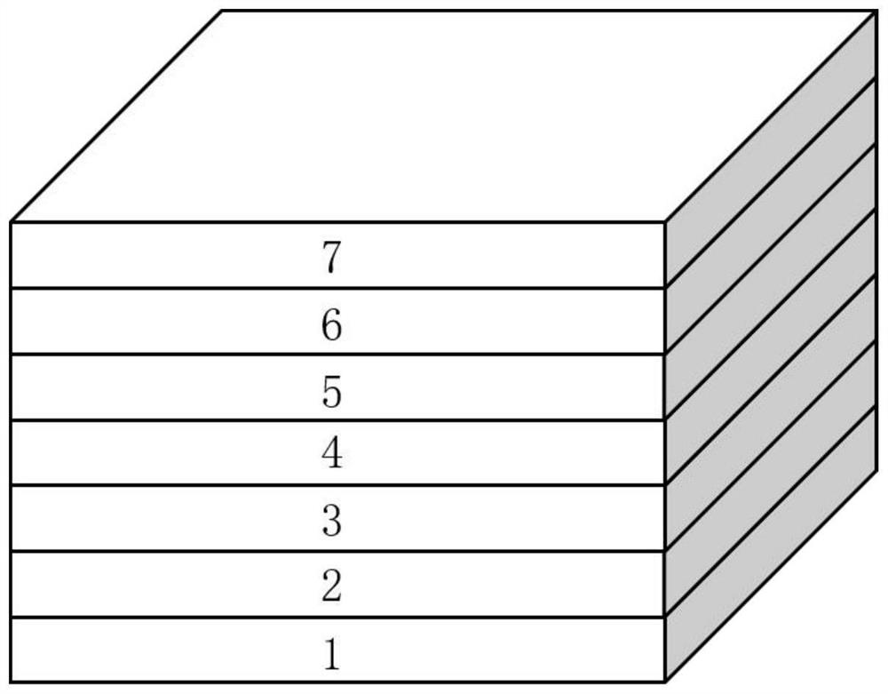
[0048] The present invention also provides a method for preparing a perovskite light-emitting diode, the steps of which are as follows:
[0049] (1) Clean the substrate
[0050] Place the glass substrate 1 with the ITO conductive film 2 in deionized water, acetone and isopropanol in sequence, ultrasonically clean it for 15-30 minutes, and then dry it;
[0051] (2) Preparation of PVK hole transport layer 3 by spin coating method
[0052] Preparation concentration is the PVK chlorobenzene solution of 5~15mg / mL, then this solution is spin-coated on the ITO conductive thin film 2 surface that step (1) obtains, and spin-coating speed is 2000~4500 rev / min, and spin-coating time is 30~ 50 seconds; then annealing at 100-150° C. for 20-40 minutes, and finally cooling to room temperature; obtaining a PVK hole transport layer 3 with a thickness of 20-40 nm;
[0053] (3) Preparation of nanoparticle and / or cryptane-doped perovskite light-emitting layer by spin coating method 4
[0054] ...
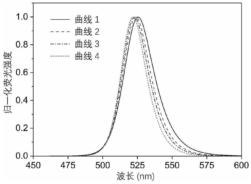
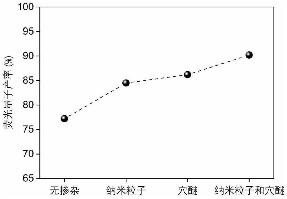
Embodiment 1
[0060] The glass substrate 1 with the ITO conductive film 2 (thickness is 100nm) is placed in deionized water, acetone and isopropanol successively, ultrasonically cleaned respectively for 20 minutes, and then dried;
[0061] Prepare a PVK chlorobenzene solution with a concentration of 10mg / mL, and then spin-coat the solution on the surface of the ITO conductive film 2 at a spin-coating speed of 4000 rpm and a spin-coating time of 40 seconds; then anneal at 120°C for 30 minutes , and finally cooled to room temperature; the obtained PVK hole transport layer 3 has a thickness of 25nm;
[0062] 0.2mmol of PbBr 2 , 0.16mmol of FABr, 0.08mmol of PEABr and 0.02mmol of CH 3 NH 3 Cl was dissolved in 0.5mL DMF and 0.5mL DMSO mixed solution, stirred at room temperature for 2 hours; then the obtained solution was spin-coated on the surface of PVK hole transport layer 3, the spin-coating speed was 7000 rpm, and the spin-coating time was 40 seconds , adding 0.15 mL of ethyl acetate drop...
Embodiment 2
[0065]The glass substrate 1 with the ITO conductive film 2 (thickness is 100nm) is placed in deionized water, acetone and isopropanol successively, ultrasonically cleaned respectively for 20 minutes, and then dried;
[0066] Prepare a PVK chlorobenzene solution with a concentration of 10mg / mL, and then spin-coat the solution on the surface of the ITO conductive film 2 at a spin-coating speed of 4000 rpm and a spin-coating time of 40 seconds; then anneal at 120°C for 30 minutes , and finally cooled to room temperature; the obtained PVK hole transport layer 3 has a thickness of 25nm;
[0067] ZrO with a grain size of 20 nm 2 The nanoparticles are dispersed in DMF, and 0.4mg / mL of ZrO 2 DMF dispersion of nanoparticles, ultrasonically dispersed for 5 hours; 0.2mmol of PbBr 2 , 0.16mmol of FABr, 0.08mmol of PEABr and 0.02mmol of CH 3 NH 3 Cl was dissolved in 0.5mL nanoparticle DMF dispersion liquid and 0.5mL DMSO mixed liquid, and stirred at room temperature for 2 hours; then t...
PUM
| Property | Measurement | Unit |
|---|---|---|
| thickness | aaaaa | aaaaa |
| thickness | aaaaa | aaaaa |
| thickness | aaaaa | aaaaa |
Abstract
Description
Claims
Application Information
 - R&D
- Intellectual Property
- Life Sciences
- Materials
- Tech Scout
- Unparalleled Data Quality
- Higher Quality Content
- 60% Fewer Hallucinations
Browse by: Latest US Patents, China's latest patents, Technical Efficacy Thesaurus, Application Domain, Technology Topic, Popular Technical Reports.
© 2025 PatSnap. All rights reserved.Legal|Privacy policy|Modern Slavery Act Transparency Statement|Sitemap|About US| Contact US: help@patsnap.com