Semiconductor laser light source module based on planar waveguide combiner and manufacturing method

A planar waveguide and laser light source technology, applied in the field of wave combiners, can solve the problems of large size, high environmental stability requirements, and increased difficulty in coupling and alignment of light sources.

Pending Publication Date: 2021-07-30
三序光学科技(苏州)有限公司
View PDF1 Cites 2 Cited by
  • Summary
  • Abstract
  • Description
  • Claims
  • Application Information

AI Technical Summary

Problems solved by technology

The structure of the optical fiber fusion tapered multiplexer is relatively simple, but it is bulky, and due to the axial loss, there are certain problems in the efficiency of the multiplexing; the structure of the spatial optical multiplexer is complex, and the adjustment is difficult. At the same time, the requirements for environmental stability are also very high, so that the overall cost is high and the volume is large; while the general PLC multiplexer is difficult to prepare high-efficiency large-channel waveguides due to the limitation of the deposition process, and the coupling is extremely difficult Big
[0004] Patent CN102967898A discloses a waveguide integrated photonic crystal combiner based on a Y-shaped curved structure, which uses a lithium niobate photonic crystal with a triangular lattice medium background air hole structure,

Method used


Image

  • Semiconductor laser light source module based on planar waveguide combiner and manufacturing method
  • Semiconductor laser light source module based on planar waveguide combiner and manufacturing method
  • Semiconductor laser light source module based on planar waveguide combiner and manufacturing method

Examples


Embodiment 1

[0053] The first manufacturing method of a semiconductor laser light source module based on a planar waveguide type combiner, comprising the following steps:

[0054] S1, the preparation of the multi-layer composite substrate of supporting substrate, bonding layer, reflective medium layer and waveguide layer: BK7 glass wafer is polished and polished, and then deposited on the lower surface by plasma chemical vapor deposition method High reflective dielectric film (reflective rate>99%); then coat bonding epoxy resin on the surface of the above-mentioned reflective medium layer and the surface of the support substrate, and then form a structure comprising the support substrate, bonding layer, reflective medium layer and waveguide layer through a resin bonding process Multi-layer composite substrate, wherein the material of the supporting substrate is Si;

[0055] S2. Wafer grinding: grinding and polishing the surface of the glass wafer in the above-mentioned multilayer composite...

Embodiment 2

[0065] The second manufacturing method of a semiconductor laser light source module based on a planar waveguide type combiner comprises the following steps:

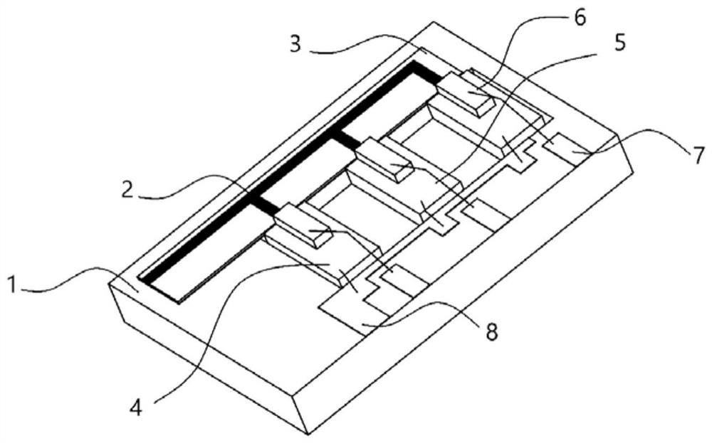
[0066] A1. Preparation of silicon-based supporting substrate containing metal layer: as Figure 9 As shown, firstly, an electrode groove 18 and an optical waveguide multiplexing structure installation groove 17 are formed on the silicon substrate 12 through an etching process, and then a laser welding metal film layer 19 and an electrode film layer 16 are formed through a deposition and etching process;

[0067] A2. Preparation of optical waveguide multiplex structure: prepare a multi-layer composite substrate including a supporting substrate, a bonding layer, a reflective medium layer and a waveguide layer by bonding and deposition processes, and then prepare an optical waveguide line pattern by grinding and etching. The waveguide multiplexing structure makes the thickness of the waveguide layer 60±5μm; finally, by cutt...


PUM

PropertyMeasurementUnit
Thicknessaaaaaaaaaa
Thicknessaaaaaaaaaa

Abstract

The invention relates to a semiconductor laser light source module based on a planar waveguide combiner, and the module comprises a bearing substrate which is provided with N electrodes; N semiconductor lasers, wherein bare chips on the semiconductor lasers are respectively bonded with the corresponding electrodes through leads; an optical waveguide combining structure sequentially comprising a waveguide layer, a reflection dielectric layer and a bonding layer from top to bottom; the waveguide layer being provided with a waveguide circuit pattern, the waveguide circuit pattern comprising N light inlets and one light outlet, and the N light inlets being in one-to-one correspondence with light outlet points of bare chips on the N semiconductor lasers; and a covering box. The invention further provides two manufacturing methods of the semiconductor laser light source module based on the planar waveguide combiner. According to the semiconductor laser light source module based on the planar waveguide type combiner provided by the invention, the large-aperture waveguide is prepared by a method of directly etching on the wafer, so that the laser coupling difficulty is greatly reduced, and the size of a device is greatly reduced.

Description

technical field [0001] The invention relates to the technical field of wave combiners, in particular to a semiconductor laser light source module and a manufacturing method based on a planar waveguide type wave combiner. Background technique [0002] With the continuous development of technology, traditional non-integrated discrete optical component systems have gradually become difficult to adapt to the development needs of contemporary information optoelectronic technology due to their shortcomings such as large volume, heavy weight, poor stability, and difficult beam coupling and alignment. In the past ten years, photonic integration based on silicon-on-insulator (Silicon-On-Insulator, SOI), lithium niobate materials, and silicon-based silicon dioxide platforms has developed rapidly. The key lies in large-area substrates and mature complementary metal oxides. Semiconductor (Complementary Metal Oxide Semiconductor, CMOS) processes are compatible, so integrated photonic dev...

Claims


Application Information

Patent Timeline
IPC IPC(8): H01S3/00G02B6/125
CPCH01S3/0071G02B6/125
Inventor 朱兵兵董英琴
Owner 三序光学科技(苏州)有限公司
Why Eureka
Try Eureka