
Acoustic surface wave transducer with multi-order transverse mode suppression and manufacturing method thereof
A surface acoustic wave and transducer technology, applied in the direction of electrical components, impedance networks, etc., can solve problems such as passband clutter, affecting the main wave mode of the original device, and affecting the Q value of the resonator
Patent Information
- Authority / Receiving Office
- CN · China
- Current Assignee / Owner
- Publication Date
- 2021-07-30
Smart Images
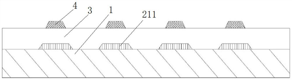
Figure 1 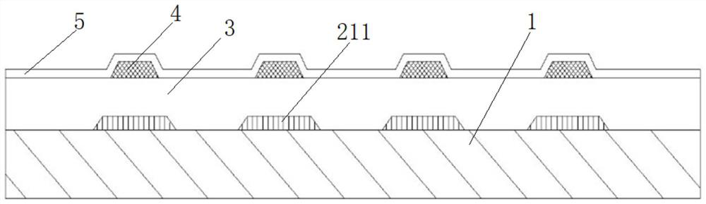
Figure 2 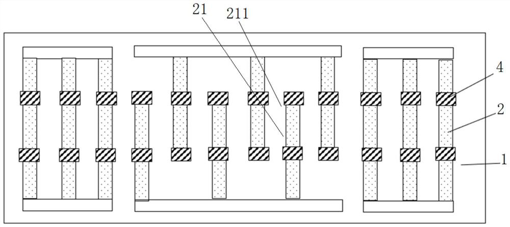
Figure 3
Abstract
Description
technical field
[0001] The invention relates to the field of surface acoustic wave devices and manufacturing techniques thereof, in particular to a multi-order transverse mode suppressed surface acoustic wave transducer and a manufacturing method. Background technique
[0002] Mobile communication has developed from the initial 2G to 3G, and then to today's 4G / 5G, frequency resources are becoming more and more crowded, and the guard interval between frequency bands of different communication systems is getting smaller and smaller. For example, for the transmitter (Tx) and receiver (Rx) duplexer frequency bands (Band2, 3, 8, 25), etc., the frequency interval between Tx and Rx is very narrow. If the frequency is changed, the frequency may drift, and Tx and Rx will affect each other, resulting in a serious deterioration of the overall performance. Therefore, temperature stability requirements are put forward for the surface acoustic wave filter as the main filter device for ra...
Examples
Embodiment 1
[0051] This embodiment discloses a surface acoustic wave transducer, which includes a wafer substrate 1, an interdigital metal layer 2, and a temperature compensation layer 3 arranged in sequence from bottom to top, and also includes a load layer 4 , the load layer 4 adopts structure one, specifically: figure 1 As shown, the load layer 4 is arranged on the upper surface of the temperature compensation layer 3, or part of the load layer 4 is embedded in the temperature compensation layer 3 and part of the temperature compensation layer 3 is exposed. Through the isolation of the temperature compensation layer 3, the load layer 4 is not separated from the interdigitated metal layer 2. Contact, not electrically connected to the interdigital metal layer 2 , the load layer 4 covers all or part of the finger bar terminals 211 in the interdigital metal layer 2 . Preferably, the load layer 4 covers all the finger ends 211 in the interdigitated metal layer 2 .
[0052] In this embodime...
Embodiment 2
[0060] This embodiment discloses a surface acoustic wave transducer. The structural principle of the surface acoustic wave transducer in this embodiment is basically the same as that of Embodiment 1. The difference is that the load layer 4 is arranged on the temperature compensation layer 3 in, such as Figure 9 and Figure 10 As shown, the load layer 4 is not in contact with the interdigital metal layer 2 , therefore, there is no risk of a short circuit between the load layer 4 and the interdigital metal layer 2 . Like the first embodiment, the load layer 4 can be a continuous strip covering a plurality of finger ends 211 or an intermittent strip covering at least one finger end 211 . Such as Figure 9 and Figure 10 As shown, the upper surface of the load layer 4 can be flush with the upper surface of the temperature compensation layer 3 ; the upper surface of the load layer 4 can also be lower than the upper surface of the temperature compensation layer 3 .
[0061] In ...
Embodiment 3
[0063] This embodiment discloses a surface acoustic wave transducer, which includes a wafer substrate 1, an interdigital metal layer 2, and a temperature compensation layer 3 arranged in sequence from bottom to top, and also includes a load layer 4, which adopts a structure of , the load layer 4 is a hollow layer arranged in the temperature compensation layer 3, the bottom of the hollow layer is not in contact with the interdigitated metal layer 2, and the hollow layer covers all or part of the finger ends 211 in the interdigitated metal layer 2, as Figure 11 and Figure 12 As shown, the upper surface of the cavity layer can be flush with the upper surface of the temperature compensation layer 3; the upper surface of the load layer 4 can also be lower than the upper surface of the temperature compensation layer 3.
[0064] In a preferred implementation of this embodiment, as Figure 12 As shown, a passivation layer 5 is also included, and the passivation layer 5 is located u...