Super-radiation light-emitting diode chip integrated with backlight detector, and preparation method thereof
A technology of superluminescent light-emitting diodes, which is applied to lasers, laser components, semiconductor lasers, etc., can solve the problems of increased ripple coefficient of superluminescent light-emitting diodes, suppress optical feedback, reduce back-end reflectivity increases, The effect of improving the ripple factor
- Summary
- Abstract
- Description
- Claims
- Application Information
AI Technical Summary
Problems solved by technology
Method used
Image
Examples
Embodiment 1
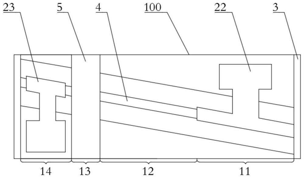
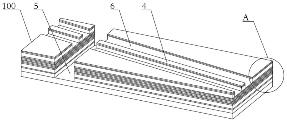
[0034] like Figure 1-3 As shown, a structural diagram of a preferred embodiment of an ultra-radiating light emitting diode chip of an integrated backlight detector, including an epitaxial piece 100, and a lower end surface of the epitaxial sheet 100 is sputtered with an N-plane electrode layer 21. The upper end surface of the formation piece 100 is sputtered with a P-plane electrode layer including an active region electrode 22 and a backlight detection zone electrode 23. The two ends of the ultra-radiation light emitting diode chip are vapor deposition film 3, which is used to increase light transmittance, reduce reflected light of the surface of the ultra-radiation light emitting diode chip, further inhibit F-P oscillation.
[0035] The upper end surface of the epitaxial piece 100 is provided with a ridge waveguide 4 in a preset angle for weight loss, inhibiting the FP oscillation; in the present embodiment, the preset angle is a ridge waveguide 4 with respect to the epitaxial. ...
Embodiment 2
[0038] like Figure 4 As shown, a flow chart of a preparation method of an ultra-radiation light emitting diode chip of an integrated backlight detector according to the present invention includes the following steps:
[0039] S1: Growth of the epiton.
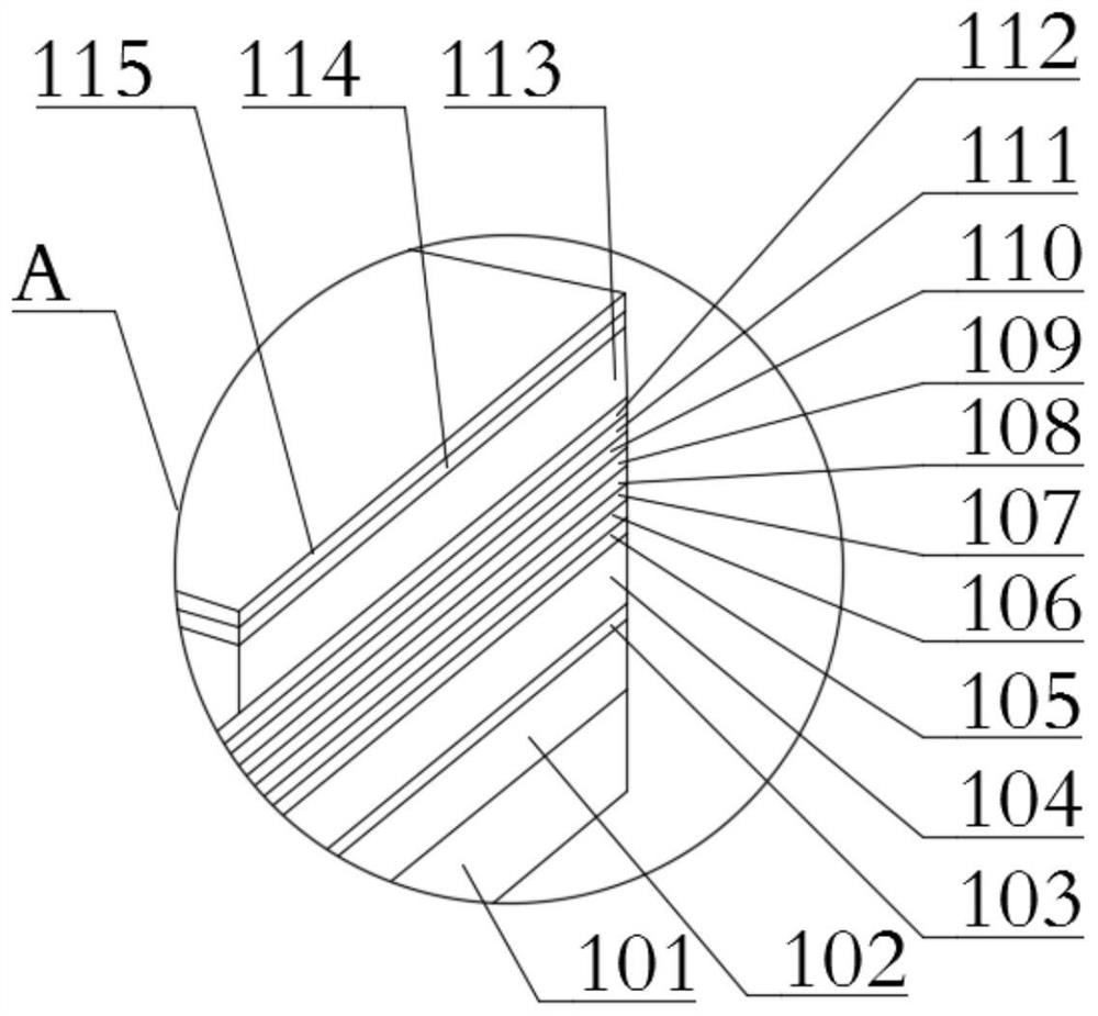
[0040] The N-INP buffer layer 102, N-INP spacer layer 104, N-AlGainas transition layer 105, N-Alinas lower limit layer 106, I- Algainas underwater wave layer 107, Algainas strain compensated multi-quantum well layer 108, I-algainas upper waveguide layer 109, p-alinas first upper limit layer 110, P-INP second upper limit layer 111, P-INGAASP corrosion termination Layer 112, P-INP third upper limit layer 113, P-INGAASP smooth layer 114 and P-INGAAS contact layer 115, result Figure 5 The epitaxial sample shown.
[0041] S2: Forming a ridge waveguide.
[0042] A layer of silica media film is deposited on the surface of the epitaxial sheet sample obtained by step S1; then the ridge waveguide 4 is photolithographed on the silica medium f...
PUM
| Property | Measurement | Unit |
|---|---|---|
| length | aaaaa | aaaaa |
| width | aaaaa | aaaaa |
| length | aaaaa | aaaaa |
Abstract
Description
Claims
Application Information


