Surface anti-reflection light-emitting diode

A technology of light-emitting diodes and anti-reflection layers, which is applied in the direction of electrical components, circuits, semiconductor devices, etc., can solve the problems of reducing process controllability and yield, increasing process complexity, increasing product costs, etc., to improve current expansion effect, anti-reflection effect is remarkable, and the effect of good precision

Inactive Publication Date: 2009-02-18
XIAMEN SANAN OPTOELECTRONICS TECH CO LTD
View PDF3 Cites 0 Cited by
  • Summary
  • Abstract
  • Description
  • Claims
  • Application Information

AI Technical Summary

Problems solved by technology

However, this process will increase the complexity of the process, reduce the controllability and yield of the process, and increase the cost of the product

Method used


Image

  • Surface anti-reflection light-emitting diode
  • Surface anti-reflection light-emitting diode
  • Surface anti-reflection light-emitting diode

Examples


Embodiment Construction

[0014] The embodiments of the present invention will be further described below in conjunction with the accompanying drawings.

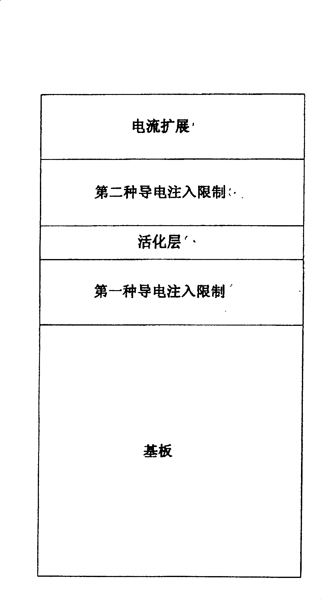
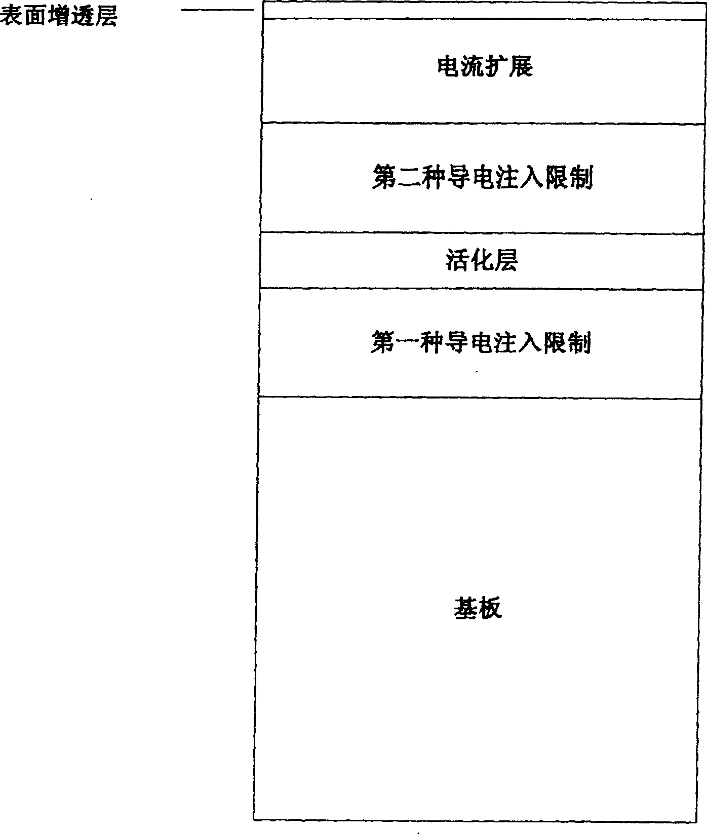
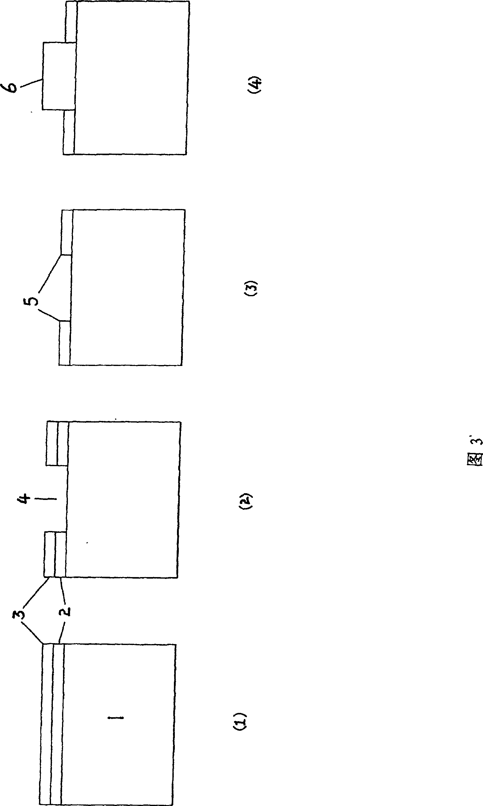
[0015] figure 1 Light-emitting diode conventional structure, figure 2 It is an epitaxial growth structure of the diode of the present invention. The typical difference between the structure of the present invention and the conventional structure is that there is a surface anti-reflection film grown in the epitaxial process on the window layer, in this example, it is AlxGa1-xAs (x=80%), and its thickness will satisfy the anti-reflection coating after oxidation. Transparent effect, such as for 625 red light emitting diodes, the thickness is 1200 angstroms. remove figure 2 structure, the surface of AlGaAs can also be covered with a protective layer such as GaAs or GaInP that is not easily oxidized (as shown in Figure 3(1), 3(2)).

[0016] Figure 3 is the process route for preparing the light emitting diode of the present invention: (a) as shown in...


PUM


Abstract

The disclosed light emitting diode (LED) adds following structure and processing to window layer in general structure: using method of chemical corrosion and oxidation turns one or multiple superficial anti reflection layers developed in epitaxy procedure to one or multiple superficial anti reflection films of aluminum suboxide; anti reflection films can be aluminum-gallium-arsenic layer or aluminum arsenide layer; there may be protection layer above anti reflection films, the protection layer can be gallium arsenide layer or gallium-indium-phosphor layer; in epitaxy procedure for LED, using metal organic chemical vapor deposition (MOCVD) completes development of structure of anti reflection films at one time. Advantages are: less reflectivity of light, and remarkable effect of anti reflection.

Description

1. Technical field [0001] The invention relates to a light-emitting diode with a surface anti-reflection film. 2. Background technology [0002] Light-emitting diodes have been used in a wide range of economic life such as display, decoration, and communication. By adopting different semiconductor materials and structures, light-emitting diodes can cover a full color range from ultraviolet to infrared, and their luminous efficiency and brightness are continuously improved. The general structure of a light-emitting diode includes a substrate, a first-type conductive carrier injection confinement layer, an active layer for controlling the emission wavelength, a second-type conductive carrier injection confinement layer, and a current spreading layer. For opaque substrates, in order to prevent light from being absorbed by the opaque substrate, a Bragg reflection layer is often inserted between the substrate and the first conductive carrier injection confinement layer to reflec...

Claims


Application Information

Patent Timeline
Patent Type & Authority Patents(China)
IPC IPC(8): H01L33/00
Inventor 何晓光黄尊祥
Owner XIAMEN SANAN OPTOELECTRONICS TECH CO LTD
Why Eureka
Try Eureka