
Two-dimensional material in-situ mechanical parameter test chip structure and preparation method thereof

A technology of mechanical parameters, two-dimensional materials, applied in the analysis of materials, material analysis using radiation, material analysis using radiation diffraction, etc., can solve the problems of small sample stage size, high price, difficulty in reducing the complexity of the sample transfer process, etc. , to achieve the effect of increasing the bearing area and reducing technical difficulties

Active Publication Date: 2021-08-10
SOUTHEAST UNIV
View PDF5 Cites 0 Cited by
  • Summary
  • Abstract
  • Description
  • Claims
  • Application Information

AI Technical Summary

Problems solved by technology

[0003] The mechanical properties under multiple static and dynamic stress loads are closely related to the formation and evolution of the internal substructure of the material, but the current research content is mainly for one-dimensional materials, and the independent static and dynamic loads under a single mode of tension or compression are established. In terms of testing, it is not possible to fully understand the mechanical properties under multiple stress loads in both tensile and compressive composite modes
Therefore, there are few reports on multiple stress loading and high-frequency dynamic loading testing techniques that can be used for transmission electron microscopy in situ tensile / compressive composite mode.
In addition, compared with one-dimensional materials, the transfer technology of two-dimensional materials to the test chip sample stage is also a huge challenge, so the structural design of the sample stage is extremely important for in-situ mechanical test chips
[0004] The existing commercial sample rods on the market include Hysitron’s PI-type nanoindentation instrument, which can realize the uniaxial tension or compression and mechanical performance testing of nanomaterials, but the experimental instrument is expensive, and a specific experimental environment must be customized , and can not achieve tensile and compression composite mode test
[0005] A mechanical test chip based on piezoelectric actuators was developed by the research group of Professor Han Xiaodong of Beijing University of Technology. This chip can realize in-situ mechanical uniaxial stretching or compression of nanomaterials, but the chip requires external driving devices and more complex related supporting equipment. , it is necessary to customize a specific TEM sample rod, and it is not possible to perform mechanical tests under tensile and compression composite modes
[0006] The aligned in-situ characterization chip developed by the research group of Wang Yuelin, Shanghai Institute of Microsystem and Information Technology, Chinese Academy of Sciences, has a structure that reduces the possibility of contamination and damage during sample preparation and transfer to the characterization chip, but the sample stage Small size makes it difficult to reduce complexity during sample transfer

Method used


Image

  • Two-dimensional material in-situ mechanical parameter test chip structure and preparation method thereof
  • Two-dimensional material in-situ mechanical parameter test chip structure and preparation method thereof
  • Two-dimensional material in-situ mechanical parameter test chip structure and preparation method thereof

Examples


Embodiment Construction

[0026] The technical solution of the present invention will be described in detail below in conjunction with the accompanying drawings.

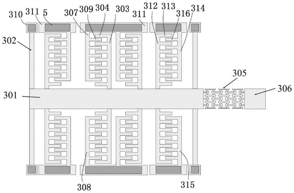
[0027] Such as figure 1 As shown, a two-dimensional material in-situ mechanical parameter test chip structure includes an electrostatic actuator, a hollow sample stage 305 and a fixed block 306;

[0028] The electrostatic actuator includes a mass block 301, the electrostatic actuator is arranged axisymmetrically with respect to the mass block 301, the mass block 301 is the symmetrical axis of the electrostatic actuator, one end of the hollow sample stage 305 is connected to the mass block 301, and the other end is connected to the fixed block 306 , the mass block 301 has the same width as the hollow sample stage 305 and the fixed block 306; the connection end between the hollow sample stage 305 and the mass block 301 moves along the axis of symmetry with the electrostatic actuator, and the connection end between the hollow sample stage 305 a...


PUM


Abstract

The invention discloses a two-dimensional material in-situ mechanical parameter test chip structure and a preparation method thereof. The chip comprises an electrostatic actuator, a hollow sample table and a fixed block, the electrostatic actuator comprises a mass block, the mass block is the symmetry axis of the electrostatic actuator, one end of the hollow sample table is connected with the mass block, the other end of the hollow sample table is connected with the fixing block, and the connecting end of the sample table and the mass block moves along the symmetry axis along with the electrostatic actuator. The connecting end, connected with the fixing block, of the hollowed-out sample table is kept still. The device is driven uniaxially and bidirectionally, and can be used for static-dynamic mechanical testing in a stretching and compressing composite mode. The hollow sample table is a bearing beam based on a concave angle honeycomb structure, so that the bearing area of the hollow sample table for carrying a sample is effectively increased, the sample transfer difficulty is reduced, and the sample is stretched or compressed.

Description

technical field [0001] The invention relates to an in-situ mechanical test chip for TEM / SEM, in particular to a structure and a preparation method of a two-dimensional material in-situ mechanical parameter test chip. Background technique [0002] In the past few decades, people have been greatly interested in the mechanical properties of two-dimensional nanomaterials. Two-dimensional materials such as graphene, graphene oxide, and molybdenum disulfide are important basic research directions because of their unique properties. Based on the special properties of bulk materials and the potential to possess unique and customizable physical properties, various nanotechnology applications including energy harvesting and storage, nanoelectromechanical systems (NEMS), flexible electronics and stretchable electronics. In addition, when the characteristic size of the material is reduced to the micro-nano scale, its mechanical properties are significantly different from those of macros...

Claims


Application Information

Patent Timeline
Patent Type & Authority Applications(China)
IPC IPC(8): G01N3/08G01N3/02G01N23/2251G01N23/04G01N23/20
CPCG01N3/08G01N3/02G01N23/2251G01N23/04G01N23/20G01N2203/0016G01N2203/0071G01N2203/0073G01N2203/0075G01N2203/0617G01N2203/0641G01N2203/0682
Inventor 聂萌黄语恒尹奎波陈姝宁
Owner SOUTHEAST UNIV
Learn More