
Power IGZO thin film transistor and preparation method thereof

A thin-film transistor and power technology, applied in transistors, semiconductor/solid-state device manufacturing, semiconductor devices, etc., can solve problems such as increased on-resistance, reduced current capability, and inability to simultaneously improve the voltage withstand capability and current capability of power devices. Achieve the effect of reducing on-resistance, enhancing controllability, and compensating for current density

Pending Publication Date: 2021-08-17
SOUTHEAST UNIV
View PDF4 Cites 0 Cited by
  • Summary
  • Abstract
  • Description
  • Claims
  • Application Information

AI Technical Summary

Problems solved by technology

However, the withstand voltage capability and current capability of power devices often cannot be improved at the same time. Resistance increases with offset distance and current capability decreases significantly

Method used


Image

  • Power IGZO thin film transistor and preparation method thereof
  • Power IGZO thin film transistor and preparation method thereof
  • Power IGZO thin film transistor and preparation method thereof

Examples


Embodiment Construction

[0028] In order to solve the above problems, the preparation method of a kind of power IGZO thin film transistor of the present invention is as follows:

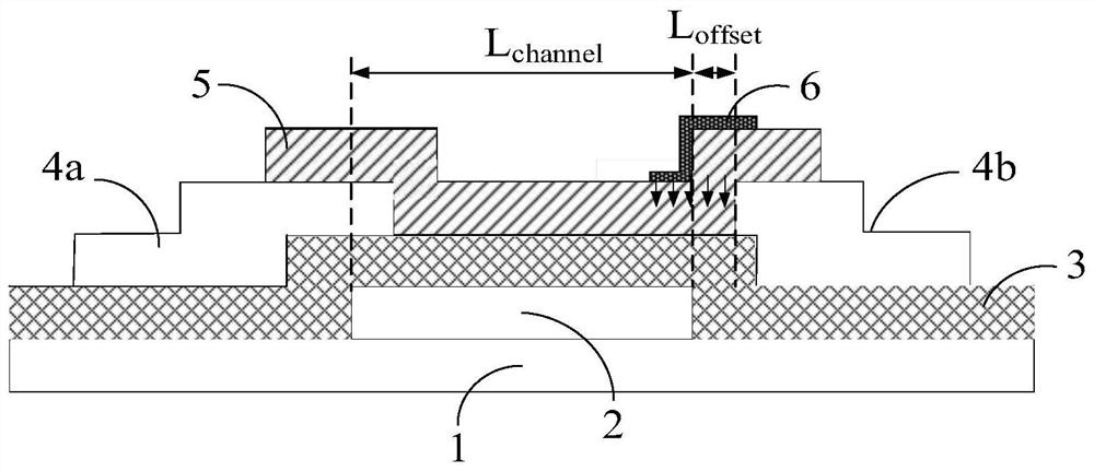
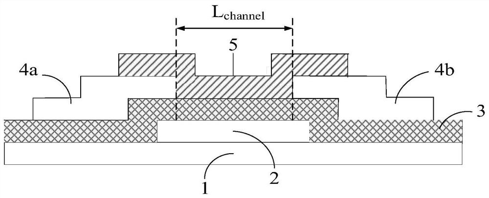
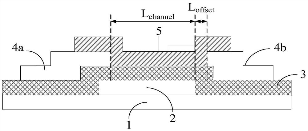
[0029] The power IGZO thin film transistor of the present invention comprises: obtaining a substrate; forming a gate electrode layer on the substrate; covering a gate insulating layer on the gate electrode layer; forming a source on one side of the gate insulating layer, A drain electrode is formed on the other side; an IGZO active layer is covered on the source electrode and the drain electrode; an Al film covering layer is formed on the IGZO active layer.

[0030] As one of the implementation methods, when depositing the source and drain metal electrodes, the overlap length of the gate electrode layer and the source electrode is 2 μm, and the offset length of the drain electrode is 2 μm through mask pattern design.

[0031] As one of the implementation methods, the Al film capping layer is arranged on the IGZO active layer...


PUM

PropertyMeasurementUnit
Widthaaaaaaaaaa
Lengthaaaaaaaaaa

Abstract

The invention provides a power IGZO thin film transistor and a preparation method thereof. The power IGZO thin film transistor comprises a substrate, a gate electrode layer, a gate insulating layer, a source electrode, a drain electrode, an IGZO layer and an Al film covering layer. In the horizontal direction, the overlapping length of the gate electrode layer and the source region electrode is 2 [mu] m, and the offset length of the gate electrode layer and the drain region electrode is 2 [mu] m. The IGZO active layer is divided into a channel region of a grid control region and an Al film covering layer of a non-grid control region in the horizontal direction, the length of the Al film covering layer is 3 microns, the overlapping length with a drain region electrode is 1 micron, and the length of a grid-drain offset region is 2 microns; and the prepared Al film covering layer is annealed for 5-10 min in the N2 atmosphere at the temperature of 300 DEG C. According to the Al film annealing process, the electron concentration of the offset region can be increased, the on-resistance of the offset region can be remarkably reduced, the working current density of the device can be improved, and the power density can be effectively improved.

Description

technical field [0001] The invention mainly relates to the technical field of power thin film transistor devices, in particular to a preparation method of a power a-IGZO thin film transistor. Background technique [0002] Indium gallium zinc oxide semiconductor (IGZO) thin films have attracted extensive attention from academia and industry due to their high mobility, low off-state current, and large-area uniformity. At present, flexible electronics is developing rapidly, and IGZO materials have attracted the attention of many researchers in flexible electronics because of their flexibility and transparency. In order to expand the application of IGZO thin film transistors in power semiconductors, it is necessary to improve the withstand voltage and current capabilities of IGZO transistors. [0003] At present, research on power IGZO thin film transistors focuses on improving withstand voltage and increasing current density. However, the withstand voltage capability and curr...

Claims


Application Information

Patent Timeline
IPC IPC(8): H01L29/786H01L21/34H01L21/477
CPCH01L29/7869H01L21/34H01L21/477H01L29/66969
Inventor 吴汪然李梦遥杨光安孙伟锋时龙兴
Owner SOUTHEAST UNIV
Features
  • Generate Ideas
  • Intellectual Property
  • Life Sciences
  • Materials
  • Tech Scout
  • Unparalleled Data Quality
  • Higher Quality Content
  • 60% Fewer Hallucinations
Learn More