Avalanche photodiode and photomultiplier detector

An avalanche photoelectric and diode technology, applied in the field of radiation detection or weak light detection, can solve the problems of large size of PMT, high working voltage, low detection efficiency, etc., and achieve the effect of improving detection efficiency and increasing range

Active Publication Date: 2021-08-17
THE SECOND ACAD OF CASIC
View PDF4 Cites 5 Cited by
  • Summary
  • Abstract
  • Description
  • Claims
  • Application Information

AI Technical Summary

Problems solved by technology

However, due to the disadvantages of large size, high working voltage, high power consumption, easy damage, low detection efficiency limited by photocath...

Method used


Image

  • Avalanche photodiode and photomultiplier detector
  • Avalanche photodiode and photomultiplier detector
  • Avalanche photodiode and photomultiplier detector

Examples


Embodiment 1

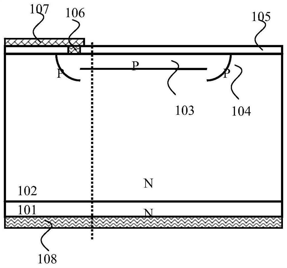
[0036] see figure 1 , which shows a schematic longitudinal section of the avalanche photodiode 201 . This embodiment is used to provide an avalanche photodiode 201 , which includes a substrate 1 and an incident light anti-reflection layer 2 . The top surface of the substrate 1 is the light incident surface, and the incident light anti-reflection layer 2 is disposed on the top surface of the substrate 1 . The incident light anti-reflection layer 2 is specifically designed according to the wavelength corresponding to the detected photons, and the material used is an anti-reflection film material such as silicon dioxide, silicon nitride or indium tin oxide.

[0037]The substrate 1 includes a plurality of doping regions, which are formed by doping the substrate 1 with impurity ions, and the method used for doping the impurity ions may be ion implantation or diffusion. The doped region includes a P-type heavily doped region 11 , an N-type heavily doped region 12 , a P-type heavil...

Embodiment 2

[0052] The embodiment of the present invention also provides a photomultiplier tube detector, such as Figure 8 As shown, the detector includes a plurality of avalanche photodiode units, and the plurality of avalanche photodiode units are connected in parallel.

[0053] Each avalanche photodiode unit includes an avalanche photodiode 201 and a quenching resistor 202 as described in Embodiment 1, and the avalanche photodiode 201 and the quenching resistor 202 are connected in series.

[0054] Anode terminals 4 of all avalanche photodiodes are connected in parallel, and cathode terminals 5 of all avalanche photodiodes are connected in parallel.

[0055] The two adjacent avalanche photodiodes 201 are respectively denoted as the first avalanche photodiode and the second avalanche photodiode, and the P-type heavily doped region 13 of the avalanche photodiode is respectively denoted as the first P-type heavily doped region and the second P-type heavily doped region. The heavily dope...


PUM

PropertyMeasurementUnit
Resistivityaaaaaaaaaa
Thicknessaaaaaaaaaa

Abstract

The invention discloses an avalanche photodiode and photomultiplier detector, relates to the technical field of radiation detection or weak light detection, and aims to solve the problem of low detection efficiency of a detector. The avalanche photodiode comprises a substrate and an incident light anti-reflection layer; the substrate comprises a plurality of doped regions, the doped regions are formed by doping foreign ions into the substrate, and the doped regions comprise a light incident end P-type heavily doped region, an N-type heavily doped region, a P-type heavily doped region, a P-type doped region and a P-type lightly doped region. The photomultiplier detector comprises a plurality of avalanche photodiode units, the plurality of avalanche photodiode units are connected in parallel, each avalanche photodiode unit comprises a quenching resistor and the avalanche photodiode involved in the technical scheme, and the avalanche photodiode and the quenching resistor are connected in series. The avalanche photodiode and the photomultiplier detector provided by the invention are used for radiation detection or weak light detection.

Description

technical field [0001] The invention relates to the technical field of radiation detection or weak light detection, in particular to an avalanche photodiode and a photomultiplier tube detector used in radiation detection or weak light detection. Background technique [0002] Low-light detector technology has always been very important in the fields of high-energy physics, astrophysics, and nuclear medical imaging. At present, the most widely used low-light detector is mainly the photomultiplier tube (PMT). However, due to the disadvantages of large size, high working voltage, high power consumption, easy damage, low detection efficiency limited by photocathode, sensitivity to magnetic field changes, and unsuitability for making large-scale detection arrays, PMT limits its application in many aspects. application. In the early 1990s, Russian scientists first proposed a detector called Silicon Photomultiplier (SiPM), which has attracted great attention from researchers in the...

Claims


Application Information

Patent Timeline
IPC IPC(8): H01L31/0352H01L31/107H01L27/146H01J43/04
CPCH01L31/035272H01L31/107H01L27/14643H01J43/04
Inventor 胡海帆秦秀波刘鹏浩赵宏鸣李志垚马喆王智斌
Owner THE SECOND ACAD OF CASIC
Why Eureka
Try Eureka