Avalanche photodiode and photomultiplier detector
An avalanche photoelectric and diode technology, applied in the field of radiation detection or weak light detection, can solve the problems of high working voltage, large size of PMT, sensitive to magnetic field changes, etc., and achieve the effect of improving the range and improving the detection efficiency.
- Summary
- Abstract
- Description
- Claims
- Application Information
AI Technical Summary
Problems solved by technology
Method used
Image
Examples
Embodiment 1
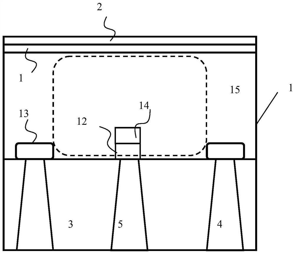
[0038] see figure 1, which shows a schematic longitudinal section of the avalanche photodiode 201 . This embodiment is used to provide an avalanche photodiode 201 , which includes a substrate 1 and an incident light anti-reflection layer 2 . The top surface of the substrate 1 is the light incident surface, and the incident light anti-reflection layer 2 is disposed on the top surface of the substrate 1 . The incident light anti-reflection layer 2 is specifically designed according to the wavelength corresponding to the detected photons, and the material used is an anti-reflection film material such as silicon dioxide, silicon nitride or indium tin oxide.
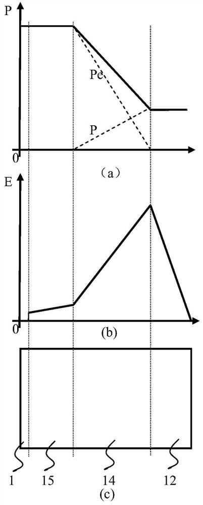
[0039] The substrate 1 includes a plurality of doping regions, which are formed by doping the substrate 1 with impurity ions, and the method used for doping the impurity ions may be ion implantation or diffusion. The doped region includes a P-type heavily doped region 11 , an N-type heavily doped region 12 , a P-type heavil...
Embodiment 2
[0053] The embodiment of the present invention also provides a photomultiplier tube detector, such as Figure 10 As shown, the detector includes a plurality of avalanche photodiode units, and the plurality of avalanche photodiode units are connected in parallel.
[0054] Each avalanche photodiode unit includes an avalanche photodiode 201 and a quenching resistor 202 as described in Embodiment 1, and the avalanche photodiode 201 and the quenching resistor 202 are connected in series.
[0055] Anode terminals 4 of all avalanche photodiodes 201 are connected in parallel, and cathode terminals 5 of all avalanche photodiodes 201 are connected in parallel.
[0056] Two adjacent avalanche photodiodes 201 are respectively marked as the first avalanche photodiode and the second avalanche photodiode, and the P-type heavily doped region 13 of the avalanche photodiode 201 is respectively marked as the first P-type heavily doped region and the second P-type heavily doped region. Type heav...
PUM
| Property | Measurement | Unit |
|---|---|---|
| electrical resistivity | aaaaa | aaaaa |
Abstract
Description
Claims
Application Information


