Supercharge Your Innovation With Domain-Expert AI Agents!

Method for forming ohmic contact to P-type silicon carbide

An ohmic contact, silicon carbide layer technology, applied in semiconductor devices, electrical components, circuits, etc., can solve problems such as expensive equipment

Pending Publication Date: 2021-08-20
HITACHI ENERGY SWITZERLAND AG
View PDF9 Cites 0 Cited by
  • Summary
  • Abstract
  • Description
  • Claims
  • Application Information

AI Technical Summary

Problems solved by technology

However, the equipment required for this ion implantation technique is specialized and expensive, and platinum is also specialized and expensive compared to aluminum

Method used


Image

  • Method for forming ohmic contact to P-type silicon carbide
  • Method for forming ohmic contact to P-type silicon carbide
  • Method for forming ohmic contact to P-type silicon carbide

Examples


Embodiment Construction

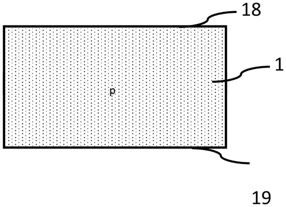
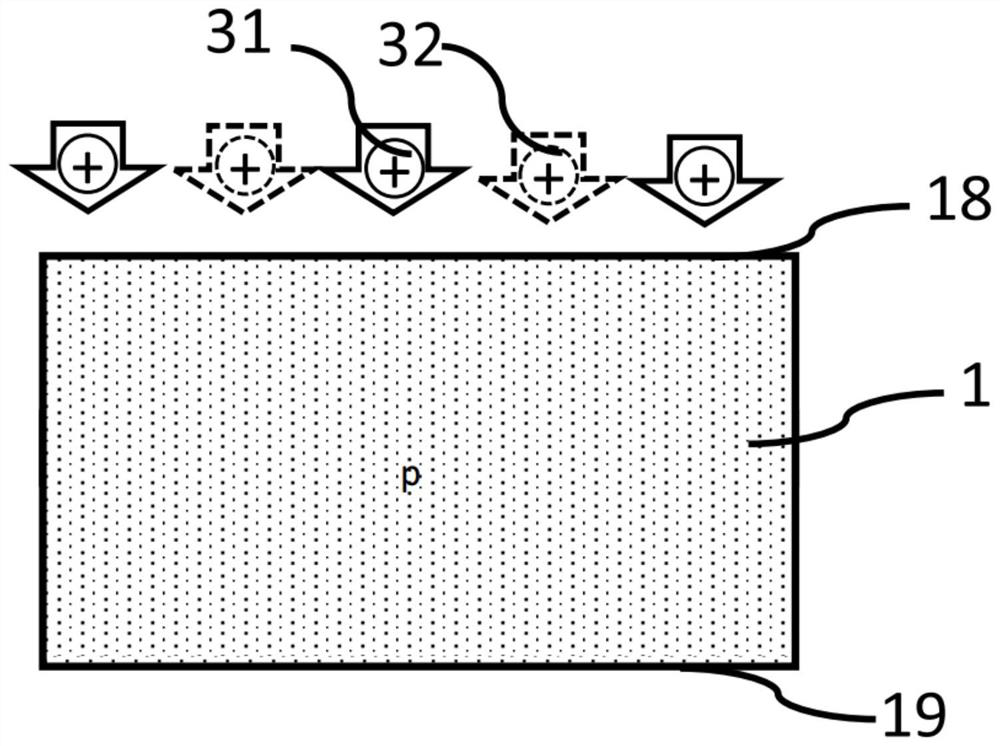
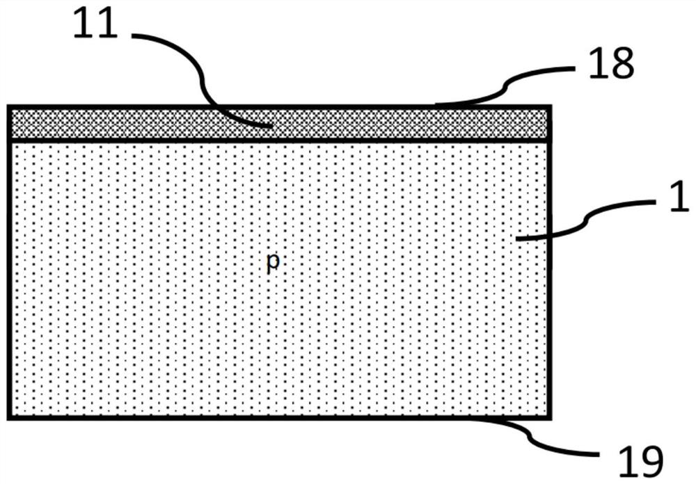
[0047] Figures 1A-1D Shown are steps of a method of forming an ohmic contact with a p-type silicon carbide layer according to an example embodiment. exist Figure 1AIn the first step shown, a p-type silicon carbide layer 1 is provided having a first main side 18 and a second main side 19 opposite to the first main side. The p-type silicon carbide layer 1 may include bulk monocrystalline and / or epitaxial layers, and may be of any polytype bulk structure, such as 4H-SiC or 6H-SiC. The p-type silicon carbide layer 1 is for example doped with aluminum and / or boron. The p-type doping of the p-type silicon carbide layer 1 can be performed by any known method, such as ion implantation, co-doping during growth by including a p-type dopant source gas in the growth chamber, in the undoped carbon Dopants are deposited (eg, by sputtering, chemical vapor deposition, evaporation, etc.) on the silicon layer followed by annealing to diffuse the dopants into the undoped silicon carbide laye...


PUM

PropertyMeasurementUnit
electron work functionaaaaaaaaaa

Abstract

A method for forming an ohmic contact to a p-type silicon carbide layer (1) comprises a step of providing the p-type silicon carbide layer (1) having a first main side (18) and a second main side (19) opposite to the first main side (18); and a step of implanting ions into the p-type silicon carbide layer (1) from the first main side (18) to form an implantation layer (11) adjacent to the first main side (18). The method is characterized in that the step of implanting the ions into the p-type silicon carbide layer (1) is performed by plasma immersion ion implantation, wherein the p-type silicon carbide layer (1) is immersed in a plasma (3) comprising first ions (31) and second ions (32), the first ions (31) being ionized aluminium atoms and the second ions (32) being different from the first ions (31).

Description

technical field [0001] The invention relates to a method for forming an ohmic contact with a p-type silicon carbide layer, in particular to a method for forming an ohmic contact with a p-type silicon carbide layer without annealing. Background technique [0002] Silicon carbide (SiC) is known to possess attractive chemical, physical and electronic properties for high-power, high-temperature and high-frequency electronic devices. In particular, higher breakdown electric field strengths in the 4H polytype structure of silicon carbide (4H-SiC) and in the 6H polytype structure of silicon carbide (6H-SiC) compared to the corresponding values ​​in silicon (Si) , higher thermal conductivity, lower intrinsic carrier concentration and higher saturation drift velocity make 4H-SiC and 6H-SiC ideal materials for power semiconductor devices. [0003] In order to be able to use silicon carbide in electronic devices or to connect such devices into electrical circuits, proper contact must ...

Claims


Application Information

Patent Timeline
Patent Type & Authority Applications(China)
IPC IPC(8): H01L21/04
CPCH01L21/0485H01L21/046H01L21/2236H01L29/1608H01L29/45H01L29/868
Inventor G·阿尔菲里V·桑达拉莫西
Owner HITACHI ENERGY SWITZERLAND AG
Features
  • R&D
  • Intellectual Property
  • Life Sciences
  • Materials
  • Tech Scout
  • Unparalleled Data Quality
  • Higher Quality Content
  • 60% Fewer Hallucinations
Learn More