Chip packaging method, chip and electronic device

A packaging method and chip technology, applied in the direction of electric solid-state devices, electrical components, semiconductor devices, etc., can solve problems such as secondary pollution, pollutant splashing, and quality degradation of intelligent power modules

Pending Publication Date: 2021-09-14
EDGELESS SEMICON CO LTD OF ZHUHAI +1
View PDF0 Cites 0 Cited by
  • Summary
  • Abstract
  • Description
  • Claims
  • Application Information

AI Technical Summary

Problems solved by technology

During the high-temperature bonding process of bonding material and copper frame on the surface of the chip, pollutants will splash onto the gate, an

Method used


Image

  • Chip packaging method, chip and electronic device
  • Chip packaging method, chip and electronic device
  • Chip packaging method, chip and electronic device

Examples


Embodiment Construction

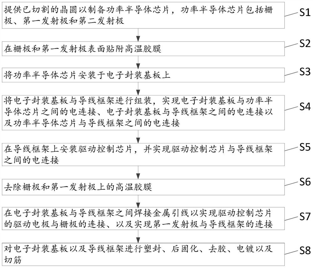
[0045] The following will clearly and completely describe the technical solutions in the embodiments of the present invention with reference to the accompanying drawings in the embodiments of the present invention. Obviously, the described embodiments are only some, not all, embodiments of the present invention. Based on the embodiments of the present invention, all other embodiments obtained by persons of ordinary skill in the art without making creative efforts belong to the protection scope of the present invention.

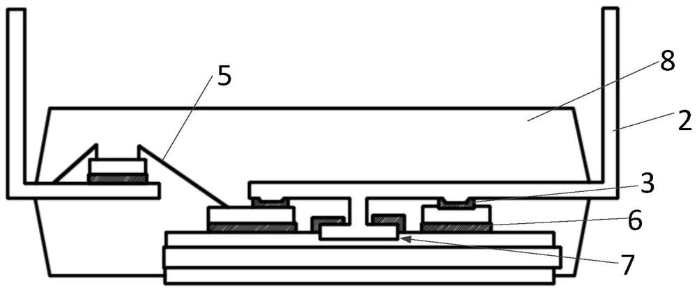
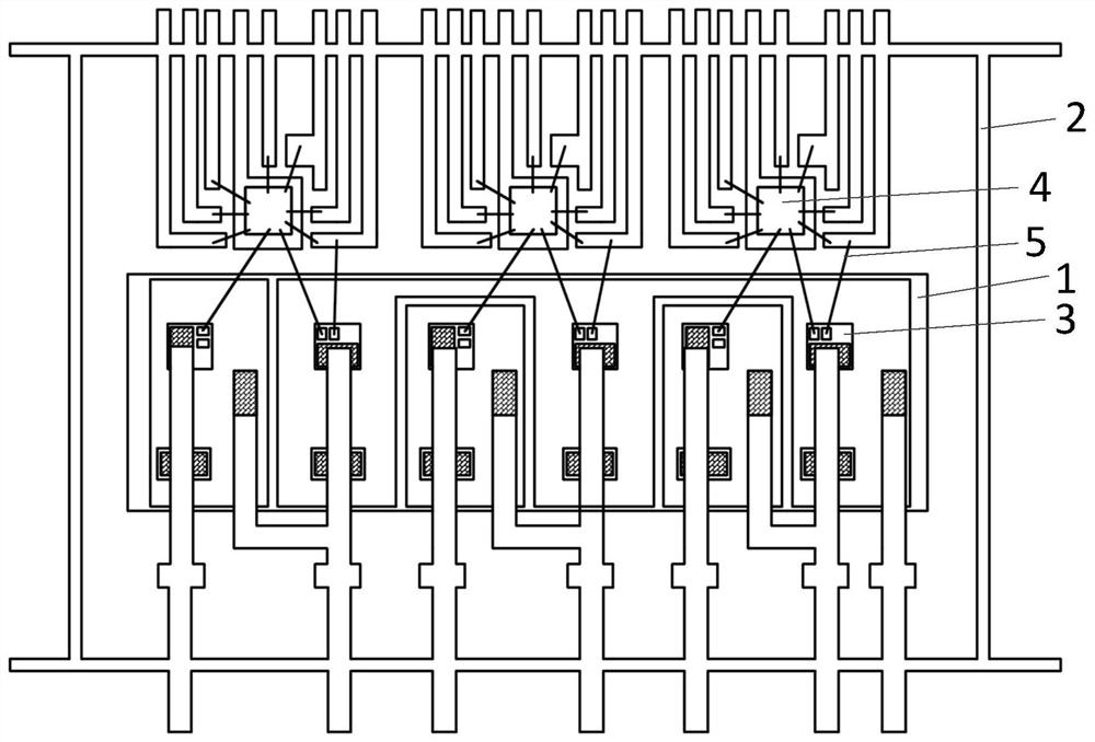
[0046] Such as figure 1 to combine image 3 and Figure 5-Figure 6 As shown, the present application provides a chip packaging method, which is used to solve the problem of polluting the grid 31 generated during the bonding process of the lead frame 2 and the chip. The specific steps are as follows:

[0047] S1: Provide a diced wafer to prepare a power semiconductor chip 3, the power semiconductor chip 3 includes a gate 31, a first emitter 32 and a second em...


PUM


Abstract

The invention relates to the technical field of intelligent power modules, and discloses a chip packaging method, a chip and an electronic device. The packaging method comprises the steps that a cut wafer is provided to prepare a power semiconductor chip, wherein the power semiconductor chip comprises a grid electrode, a first emitting electrode and a second emitting electrode; high-temperature adhesive films are attached to the surfaces of the grid electrode and the first emitting electrode; the power semiconductor chip is mounted on the electronic packaging substrate; the electronic packaging substrate and a lead frame are assembled to realize electric connection between all the components; a driving control chip is mounted on the lead frame, and electric connection is realized; the high-temperature adhesive films are removed; the connection between the driving electrode of the driving control chip and the grid electrode and the connection between the first emitting electrode and the lead frame are realized; and plastic packaging, post-curing, photoresist removal, electroplating and rib cutting are carried out. According to the packaging method disclosed by the invention, the problem of grid pollution generated in the combination process of the lead frame and the chip can be prevented, and the reliability of the grid bonding wire is enhanced.

Description

technical field [0001] The present application relates to the technical field of intelligent power modules, in particular to a chip packaging method, a chip and an electronic device. Background technique [0002] The intelligent power module not only integrates the power switching device and the driving circuit, but also has built-in fault detection circuits such as overvoltage, overcurrent and overheating, and can send detection signals to the CPU. It is composed of a high-speed and low-power die, an optimized gate drive circuit and a fast protection circuit, which can ensure that the intelligent power module itself is not damaged even if a load accident or improper use occurs. With the further increase of the current density of power devices, higher requirements are put forward for the heat dissipation capabilities of devices and modules, and the market requires increasingly light, thin, short, small and low-cost products, and the miniaturization of power devices or module...

Claims


Application Information

Patent Timeline
IPC IPC(8): H01L21/48H01L21/56H01L23/495H01L25/18
CPCH01L23/49548H01L23/49575H01L25/18H01L21/4825H01L21/56H01L2224/48137H01L2224/48247
Inventor 江伟史波曾丹敖利波肖婷曹俊马颖江
Owner EDGELESS SEMICON CO LTD OF ZHUHAI
Why Eureka
Try Eureka