Module processing method, module and device

A processing method and module technology, applied in the field of electronics, can solve the problems of difficult flip-chip soldering, solder collapse, short circuit between the chip and the circuit board bridge, etc.

Active Publication Date: 2021-09-14
FOSHAN NATIONSTAR OPTOELECTRONICS CO LTD
View PDF9 Cites 1 Cited by
  • Summary
  • Abstract
  • Description
  • Claims
  • Application Information

AI Technical Summary

Problems solved by technology

Although flip chip soldering saves the wire bonding process and improves the heat dissipation performance between the circuit board and the chip, there are still some difficulties in flip chip soldering
After the flip chip is mounted on the circuit board by solder, the solder will go through four stages of preheating, activation, reflow and cooling when passing through the reflow furnace. The easily volatile components in the flux cannot volatilize in an orderly manner, so the solder particles are extruded, causing the solder to collapse. The collapse of the solder will shorten or stabilize the distance between the chip and the circuit board, resulting in insufficient bonding between the chip and the circuit board or There is a bridge between the chip and the circuit board to form a short circuit; during the reflow and cooling stages, some of the flux that has not been volatilized in time will be wrapped in the molten solder, and after the solder cools and solidifies, voids will appear between the soldering layer of the chip and the circuit board , the formation of voids will reduce the effective interconnection area of ​​the solder layer, resulting in insufficient bonding force between the chip and the circuit board

Method used


Image

  • Module processing method, module and device
  • Module processing method, module and device
  • Module processing method, module and device

Examples


Embodiment Construction

[0045] The following will clearly and completely describe the technical solutions in the embodiments of the present invention with reference to the accompanying drawings in the embodiments of the present invention. Obviously, the described embodiments are only some, not all, embodiments of the present invention. Based on the embodiments of the present invention, all other embodiments obtained by persons of ordinary skill in the art without creative efforts fall within the protection scope of the present invention.

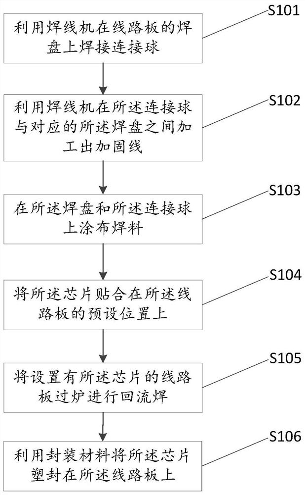
[0046] figure 1 It is a flow chart of a module processing method according to an embodiment of the present invention.

[0047] An embodiment of the present invention provides a module processing method, including:

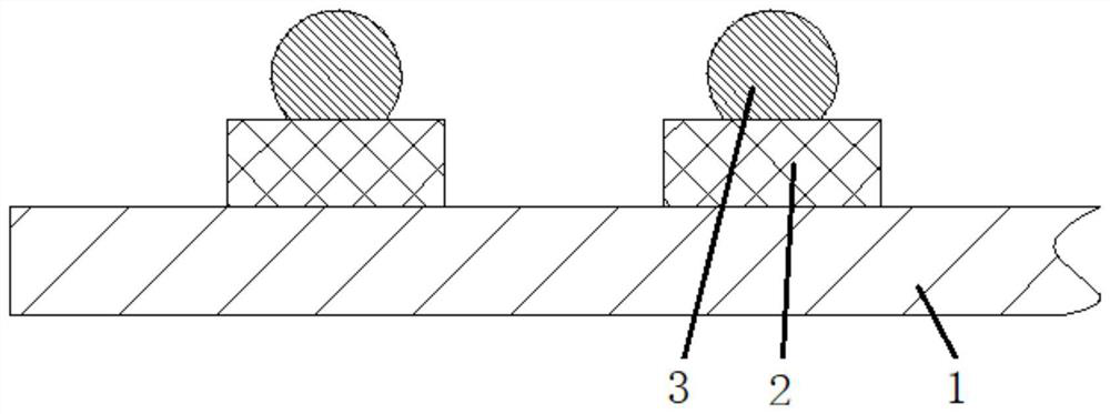
[0048] S101: Solder the connection ball 3 on the pad 2 of the circuit board 1 by using a wire bonding machine;

[0049] figure 2 It is a schematic diagram of the semi-finished module structure after soldering the connection ball.

[0050] Specifica...


PUM


Abstract

The invention provides a module processing method, module and device. The module processing method comprises the following steps: welding a connecting ball on a bonding pad of a circuit board by using a wire bonding machine; coating the bonding pad and the connecting ball with solder; attaching a chip to a preset position of the circuit board; carrying out reflow soldering on the circuit board provided with the chip through a furnace to make the electrode of the chip, the connecting ball, the solder and the bonding pad jointed; and plastic-packaging the chip on the circuit board by using a packaging material, and enabling the packaging material, the chip and the circuit board to form the module. According to the module processing method, the chip is fixed after the connecting ball is welded on the bonding pad of the circuit board, so that the binding force between the chip and the circuit board can be effectively improved, and the use reliability of the module and the device is ensured.

Description

technical field [0001] The invention relates to the field of electronics, in particular to a module processing method, a module and a device. Background technique [0002] In recent years, flip-chip bonding technology has become an important direction of semiconductor packaging. Commonly used flip chip welding is mainly to bond the electrodes of the flip chip to the pads of the circuit board through solder to realize the electrical connection between the flip chip and the circuit board. Although the soldering of the flip chip saves the wire bonding process and improves the heat dissipation performance between the circuit board and the chip, there are still some difficulties in the soldering of the flip chip. After the flip chip is mounted on the circuit board by solder, the solder will go through four stages of preheating, activation, reflow and cooling when passing through the reflow furnace. The easily volatile components in the flux cannot volatilize in an orderly manne...

Claims


Application Information

Patent Timeline
Patent Type & Authority Applications(China)
IPC IPC(8): H05K3/40H05K1/11H05K1/18H05K13/04
CPCH05K3/4015H05K1/111H05K13/0465H05K1/181
Inventor 李年谱李碧波秦快郭恒赵强李红王军永陈红文欧阳小波
Owner FOSHAN NATIONSTAR OPTOELECTRONICS CO LTD
Why Eureka
Try Eureka