Cylindrical crystal oscillator and chip individual packaging structure based on multi-layer embedded substrate

A multi-layer substrate and packaging structure technology, applied in electrical components, impedance networks, etc., can solve the problems of complex packaging process, difficult SMT welding, affecting yield, etc., to avoid mold processing costs, short processing cycles, and flexible design. Effect

Pending Publication Date: 2021-09-21
BEIJING 7Q TECH
View PDF0 Cites 0 Cited by
  • Summary
  • Abstract
  • Description
  • Claims
  • Application Information

AI Technical Summary

Problems solved by technology

The biggest deficiency and disadvantage of this kind of crystal oscillator and chip integrated package is that the packaging process is complicated, the traditional cylindrical crystal oscillator with a frequency of 26.768KHz is bulky, and it is not easy to be soldered on the package frame by SMT (surface mount), and it is necessary to use a special cylindrical crystal oscillator lead to bend machine, installation machine and manual welding, affecting the yield and high cost, packaging cost

Method used


Image

  • Cylindrical crystal oscillator and chip individual packaging structure based on multi-layer embedded substrate
  • Cylindrical crystal oscillator and chip individual packaging structure based on multi-layer embedded substrate
  • Cylindrical crystal oscillator and chip individual packaging structure based on multi-layer embedded substrate

Examples


Embodiment Construction

[0026] Exemplary embodiments of the present disclosure will be described in more detail below with reference to the accompanying drawings. Although exemplary embodiments of the present disclosure are shown in the drawings, it should be understood that the present disclosure may be embodied in various forms and should not be limited by the embodiments set forth herein. Rather, these embodiments are provided for more thorough understanding of the present disclosure and to fully convey the scope of the present disclosure to those skilled in the art.

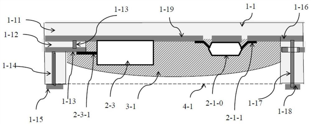
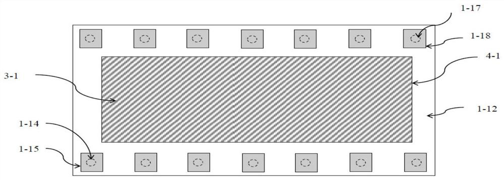
[0027] The present invention utilizes the traditional low-cost PCB multilayer substrate to design a single package structure of columnar crystal oscillator and chip based on the multilayer concave embedded substrate. The bulk crystal electrode wire can be installed and welded on the step layer substrate electrode without bending. The inner and outer layers are designed to use the PCB substrate as a flexible wiring connection method...


PUM


Abstract

The invention relates to a cylindrical crystal oscillator and chip individual packaging structure based on a multi-layer embedded substrate. The cylindrical crystal oscillator and chip individual packaging structure comprises a multi-layer substrate, a multi-layer substrate signal line, a multi-layer substrate ground line, a bottom electrode and a grounding electrode, wherein the lower surface of the multi-layer substrate is provided with an embedding space; at least one cylindrical crystal oscillator and at least one crystal oscillator driving chip are horizontally arranged in the embedding space; a step-shaped structure is formed in the space; the cylindrical crystal oscillator is horizontally arranged on an inner-layer substrate base of the embedding space of the multi-layer substrate; a chip is soldered to the inner-layer substrate base of the embedding space of the multi-layer substrate; the multi-layer substrate is provided with the step-shaped structure in the embedding space; a lead electrode of the cylindrical crystal oscillator is smoothly soldered with a substrate electrode on the step-shaped structure without bending; the substrate electrode is connected with the bottom layer electrode through the multi-layer substrate signal line; and the cylindrical crystal oscillator is connected with the crystal oscillator driving chip through a multi-layer substrate connecting line. The structure is short in processing period and low in cost.

Description

technical field [0001] The invention relates to the technical field of multi-device packaging design using a substrate, in particular to a single package structure of a cylinder crystal oscillator and a chip based on a multi-layer recessed embedded substrate. Background technique [0002] So far, many devices and terminals related to electronic information systems need local clock devices. The combination of crystals and clock chips can provide stable digital pulse signals and time. According to the application, in many occasions where time data is generated at present, the crystal oscillator and the chip are separated, and the crystal oscillator is installed next to the chip, but the crystal and the chip are connected through the PCB master. Dust, the dust on the pin angle connection of these devices will form a tiny parasitic capacitance, which will affect the oscillation period of the crystal oscillator for a long time. When combined with the clock chip, time drift will o...

Claims


Application Information

Patent Timeline
Patent Type & Authority Applications(China)
IPC IPC(8): H03H9/02
CPCH03H9/02
Inventor 不公告发明人
Owner BEIJING 7Q TECH
Why Eureka
Try Eureka