Base material with high surface binding force and preparation method thereof
A technology with high bonding force and high surface, applied in welding equipment, manufacturing tools, laser welding equipment, etc., can solve problems such as complex process, environmental pollution by chemical methods, and small application range of coarsening formula, so as to change the hydrophilicity and hydrophobicity, and the application range Wide, simple and clear effect of adjustment process
- Summary
- Abstract
- Description
- Claims
- Application Information
AI Technical Summary
Problems solved by technology
Method used
Image
Examples
Embodiment 1
[0041]The material selected in this embodiment is an LCP thin film insulating material with a film thickness of 100 μm, which needs to be plated with copper on the surface, and sandblasting will deform or damage the material. LCP itself has good chemical resistance, but chemical roughening is difficult.
[0042] A method for preparing a substrate with high surface binding force, the method comprising the steps of:
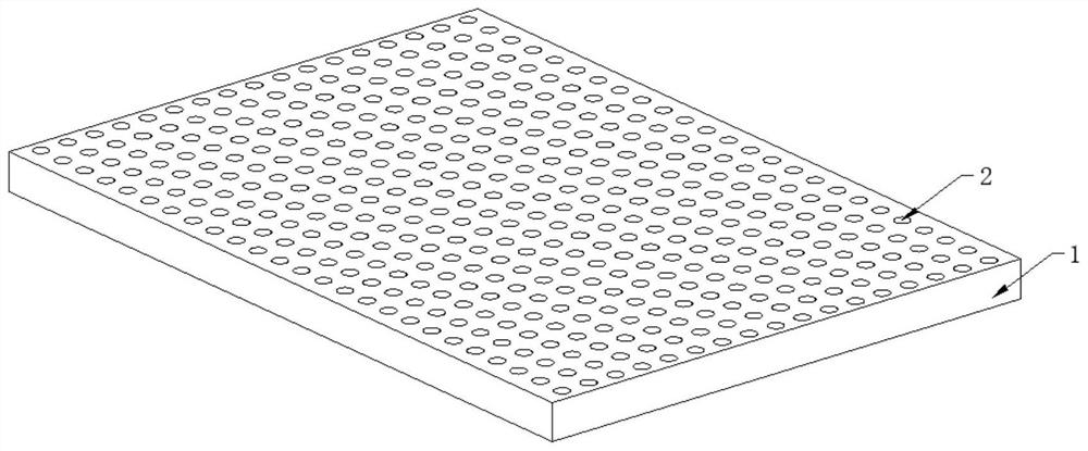
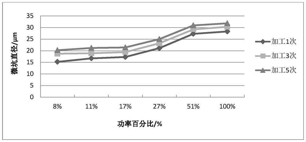
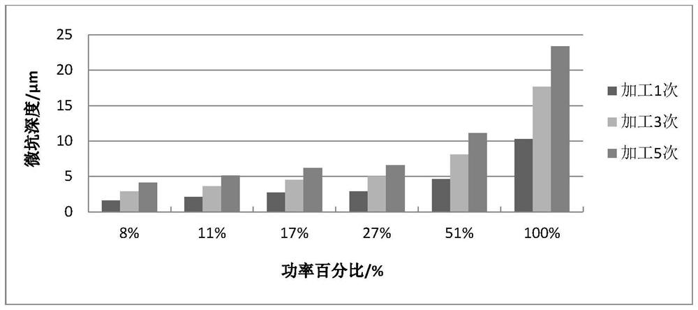
[0043] 1) Laser selection: use different types of pulsed lasers to scan the surface of the substrate (1) in the form of a single pulse laser beam, and form micropits (2) on the surface, and measure the diameter of the micropits (2) formed on the substrate Size and depth, and select the type of pulsed laser that can react with the surface of the substrate;
[0044] In this embodiment, the DirectLaser 550U ultraviolet nanosecond laser machine produced by Dezhong (Tianjin) Technology Development Co., Ltd. is preferably used to carry out the laser processing test.
...
Embodiment 2
[0063] The material selected in this embodiment is an FR4 insulating material with a thickness of 0.5 mm, and copper plating and copper plating are required on the surface. After the material is roughened by plasma treatment or traditional degumming methods such as potassium permanganate, foaming problems will occur when copper is deposited. Enhanced treatment conditions, or a combination of the two treatment methods, copper sinking does not bubble, but is directly delaminated after copper plating.
[0064] 1) Laser selection: use different types of pulsed lasers to scan the surface of the substrate (1) in the form of a single pulse laser beam, and form micropits (2) on the surface, and measure the diameter of the micropits (2) formed on the substrate Size and depth, and select the type of pulsed laser that can react with the surface of the substrate;
[0065] In this embodiment, the DirectLaser 550U ultraviolet nanosecond laser machine produced by Dezhong (Tianjin) Technolog...
PUM
| Property | Measurement | Unit |
|---|---|---|
| wavelength | aaaaa | aaaaa |
| surface roughness | aaaaa | aaaaa |
| thickness | aaaaa | aaaaa |
Abstract
Description
Claims
Application Information


