
QFN packaging semiconductor device

A semiconductor and device technology, which is applied in the field of QFN packaged semiconductor devices, can solve problems such as oversized pads and short circuits, and achieve the effects of controlling short circuits, improving cross-linking density, and good mechanical properties

Active Publication Date: 2021-09-28
XIAN HANGSI SEMICON CO LTD
View PDF7 Cites 0 Cited by
  • Summary
  • Abstract
  • Description
  • Claims
  • Application Information

AI Technical Summary

Problems solved by technology

[0003] The conventional QFN package design in the PCB usually has a large-area heat dissipation pad, which is usually grounded. Although this heat dissipation pad can play the role of chip heat dissipation, it is often too large to Too much tin brushing during the (SMT) process will cause a short circuit between the large heat dissipation pad in the center of the QFN package and other small conductive pads
In addition, with the continuous development of integrated circuit packaging towards high density, high integration, and high speed, the packaging structure is also facing a series of reliability risks caused by chip heating.

Method used


Image

  • QFN packaging semiconductor device
  • QFN packaging semiconductor device
  • QFN packaging semiconductor device

Examples


Embodiment

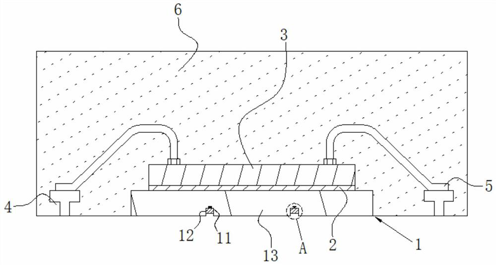
[0021] Embodiment: a kind of QFN encapsulation semiconductor device, comprise and be positioned at heat radiation pad 1, chip 3 and conductive pad 4 in epoxy insulator 6, described chip 3 is positioned on heat radiation pad 1, and described chip 3 and heat radiation welding A silver paste layer 2 is provided between the disks 1, and several conductive pads 4 are provided around the heat dissipation pad 1, and the conductive pads 4 and the chip 3 are connected by a lead 5;

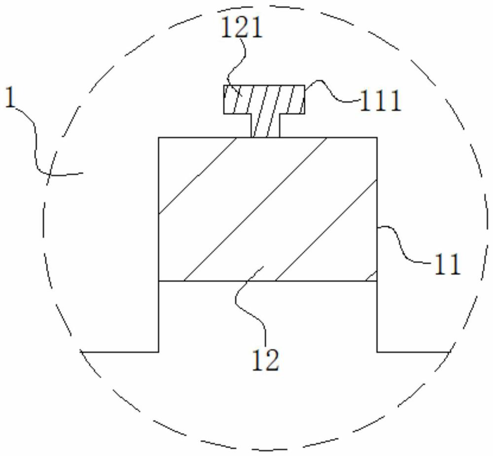
[0022] The side of the heat dissipation pad 1 away from the chip 3 is provided with a separation groove 11, the width of the separation groove 11 is 0.1-0.3 mm, and the separation groove 11 divides the side of the heat dissipation pad 1 away from the chip 3 into equal parts. At least two single pads 13, the separation grooves 11 are filled with heat-conducting insulating strips 12, the walls of the separation grooves 11 are provided with several T-shaped grooves 111 extending into the heat dissipation pads 1...


PUM

PropertyMeasurementUnit
glass transition temperatureaaaaaaaaaa

Abstract

The invention discloses a QFN packaging semiconductor device, which comprises a heat dissipation bonding pad, a chip and a conductive bonding pad positioned in an epoxy insulator. One side, far away from the chip, of the heat dissipation bonding pad is provided with a separation groove, the width of the separation groove is 0.1-0.3 mm, and the separation groove equally divides the side, far away from the chip, of the heat dissipation bonding pad into at least two bonding pad monomers; the epoxy insulator is prepared from the following raw material components in parts by weight: epoxy resin, linear phenolic resin, liquid nitrile rubber, diphenylmethane diisocyanate, diethyl pyrocarbonate, dibenzyl phosphate, silica powder, gamma-methacryloxypropyltrimethoxysilane, 5-fluoro-2-methoxyaniline, 2, 4, 6-tri (dimethylaminomethyl) phenol, a release agent and a flame retardant. According to the QFN packaging semiconductor device, the overall mechanical property of the epoxy insulator is enhanced, and the stability of a packaging structure is effectively guaranteed.

Description

technical field [0001] The invention belongs to the technical field of leadless packaging, and in particular relates to a QFN packaging semiconductor device. Background technique [0002] QFN packaging is widely used in PCB boards, and the application of QFN packaging has greatly promoted the development of electronic technology. The QFN package has excellent thermal performance, mainly because there is a large area of ​​heat dissipation soldering at the bottom of the package. In order to effectively conduct heat from the chip to the PCB, the bottom of the PCB must be designed with corresponding heat dissipation pads and heat dissipation vias. The pad provides a reliable soldering area, and the thermal via provides a heat dissipation path. [0003] The conventional QFN package design in the PCB usually has a large-area heat dissipation pad, which is usually grounded. Although this heat dissipation pad can play the role of chip heat dissipation, it is often too large to Too...

Claims


Application Information

Patent Timeline
Patent Type & Authority Applications(China)
IPC IPC(8): H01L23/31H01L23/29H01L23/48H01L23/367H01L23/498
CPCH01L23/293H01L23/367H01L23/488H01L2924/181H01L2224/73265H01L2224/48247H01L2224/48465H01L2924/00012
Inventor 马磊党鹏杨光彭小虎王新刚庞朋涛任斌王妙妙
Owner XIAN HANGSI SEMICON CO LTD
Learn More