Fully-depleted silicon-on-insulator substrate, transistor and preparation method and application thereof

A silicon-on-insulator and fully depleted technology, which is applied in semiconductor/solid-state device manufacturing, semiconductor devices, electrical components, etc., can solve problems such as complex process flow of FinFET devices, difficult SOI substrate, and process cost reduction, and achieve the goal of suppressing substrate Bottom pulse current interference, reduced leakage, and simple process

Pending Publication Date: 2021-10-01
GUANGDONG GREATER BAY AREA INST OF INTEGRATED CIRCUIT & SYST
View PDF0 Cites 0 Cited by
  • Summary
  • Abstract
  • Description
  • Claims
  • Application Information

AI Technical Summary

Problems solved by technology

[0002] As its core device, the non-planar Fin FET device structure has strong gate control ability and strong ability to suppress the short channel effect, but the process flow of the Fin FET device is complicated; compared with the three-dimensional Fin FET process, the planar SOI device process The number of photolithography plates is much less, the process is relatively easier, and the process cost is greatly reduced
However, how to fabricate SOI substrates with small parasitic capacitance and low leakage is still a difficult point

Method used


Image

  • Fully-depleted silicon-on-insulator substrate, transistor and preparation method and application thereof
  • Fully-depleted silicon-on-insulator substrate, transistor and preparation method and application thereof
  • Fully-depleted silicon-on-insulator substrate, transistor and preparation method and application thereof

Examples


Embodiment

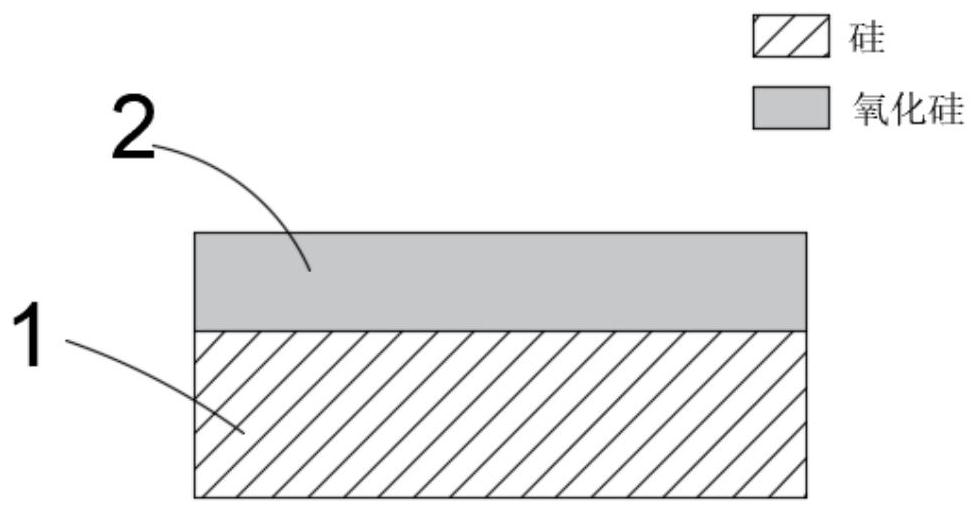
[0037] In the first step, a silicon oxide layer 2 is formed on the backing silicon layer 1 to obtain the following figure 1 The shape shown.

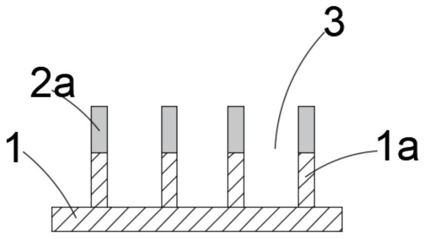
[0038] In the second step, photolithography and etching are carried out to form a plurality of grooves 3 in the silicon oxide layer 2, and obtain the following figure 2 The shape shown. Wherein, the trench 3 penetrates the silicon oxide layer 2 and goes deep into the backing silicon layer 1, so that the surface of the backing silicon layer 1 is divided into a plurality of silicon lines 1a, and the silicon oxide layer 2 is divided into a plurality of silicon oxide lines 2a. , the aspect ratio of the trench 3 is above 2:1, and the width of each of the silicon lines 1 a and the silicon oxide lines 2 a is 10 nm˜100 nm.

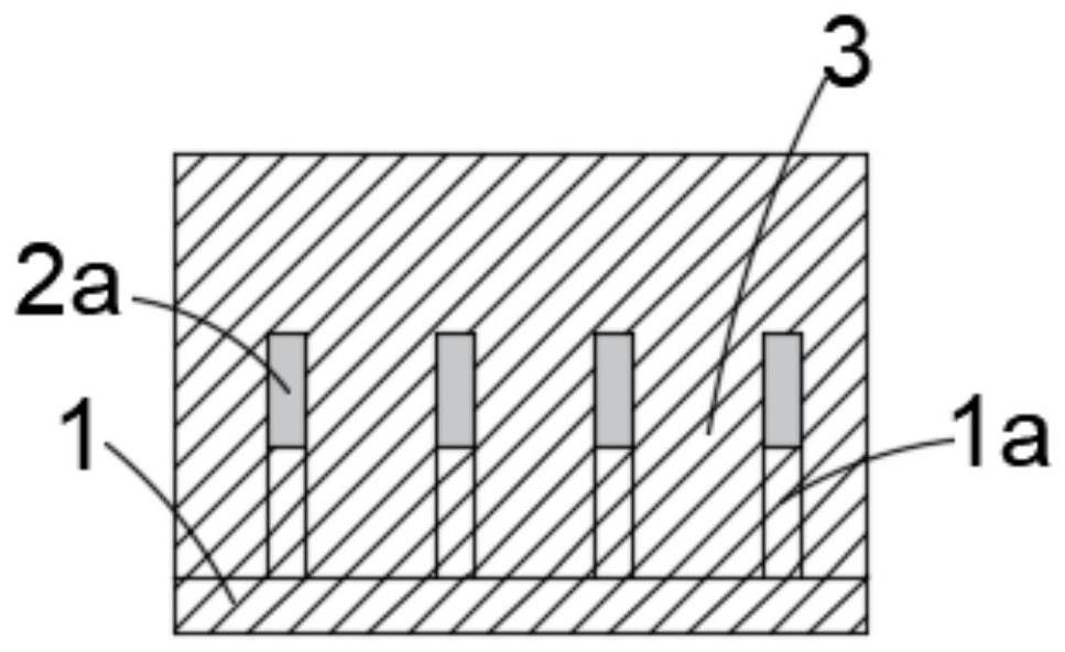
[0039] In the third step, the silicon top layer 3 is formed by selective epitaxial growth, and the following image 3 The shape shown.

[0040] The fourth step is to thin the silicon top layer 3 to obtain such as Fi...


PUM

PropertyMeasurementUnit
widthaaaaaaaaaa

Abstract

The invention relates to a fully-depleted silicon-on-insulator substrate, a transistor and a preparation method and an application thereof. The preparation method of the fully-depleted silicon-on-insulator substrate comprises the following steps: forming a silicon oxide layer on a back lining silicon layer; carrying out photoetching and etching to enable the silicon oxide to form a plurality of grooves, enabling the grooves to penetrate through the silicon oxide layer and penetrate into the back lining silicon layer, enabling the surface of the back lining silicon layer to be divided into a plurality of silicon lines, and enabling the silicon oxide layer to be divided into a plurality of silicon oxide lines; forming a silicon top layer, wherein the silicon top layer fills the groove and covers the silicon oxide lines; thinning the silicon top layer; coating photoresist on the surface of the silicon top layer, and patterning to expose the surface of the silicon top layer covering the silicon oxide lines and the spacing areas of the adjacent silicon oxide lines; carrying out oxygen injection; and then annealing to form a silicon oxide isolation layer. According to the manufactured substrate, a parasitic capacitance can be reduced, and the operation speed can be increased; electric leakage can be reduced, and power consumption is lower; the latch-up effect can be eliminated; the substrate pulse current interference can be inhibited; and meanwhile, a strain is introduced.

Description

technical field [0001] The invention relates to the field of semiconductor production technology, in particular to a fully depleted silicon-on-insulator substrate, a transistor and a preparation method thereof. Background technique [0002] As its core device, the non-planar Fin FET device structure has strong gate control ability and strong ability to suppress the short channel effect, but the process flow of the Fin FET device is complicated; compared with the three-dimensional Fin FET process, the planar SOI device process The number of photoresist plates is much less, the process is relatively easier, and the process cost is greatly reduced. However, how to manufacture SOI substrates with small parasitic capacitance and low leakage is still a difficult point. [0003] For this reason, the present invention is proposed. Contents of the invention [0004] The main purpose of the present invention is to provide a method for preparing a fully depleted silicon-on-insulato...

Claims


Application Information

Patent Timeline
Patent Type & Authority Applications(China)
IPC IPC(8): H01L29/78H01L29/06H01L21/336
CPCH01L29/7855H01L29/0603H01L29/0684H01L29/66795H01L21/7624
Inventor 亨利·H·阿达姆松王桂磊戚璇王云叶甜春
Owner GUANGDONG GREATER BAY AREA INST OF INTEGRATED CIRCUIT & SYST
Why Eureka
Try Eureka