Semiconductor structure and forming method of semiconductor structure

A semiconductor and structured surface technology, applied in semiconductor devices, semiconductor/solid-state device manufacturing, electrical components, etc., to improve performance, reduce capillary force, and improve flatness

Pending Publication Date: 2021-10-12
SEMICON MFG INT (SHANGHAI) CORP +1
View PDF0 Cites 1 Cited by
  • Summary
  • Abstract
  • Description
  • Claims
  • Application Information

AI Technical Summary

Problems solved by technology

However, when the feature size (CD, Critical Dimension) of the device is further reduced, even if the gate-last process is adopted, the structure of the conventional metal-oxide semiconductor field-effect transistor (MOSFET) can no longer meet the requirements for device performance. devices have received widespread attention as replacements for conventional

Method used


Image

  • Semiconductor structure and forming method of semiconductor structure
  • Semiconductor structure and forming method of semiconductor structure
  • Semiconductor structure and forming method of semiconductor structure

Examples


Embodiment Construction

[0029] As mentioned in the background, the performance of semiconductor devices still needs to be improved. Now analyze and illustrate in conjunction with specific embodiment.

[0030] It should be noted that the "surface" in this specification is used to describe the relative positional relationship in space, and is not limited to direct contact.

[0031] Figure 1 to Figure 4 It is a schematic cross-sectional structure diagram of each formation step in the formation process of a semiconductor structure.

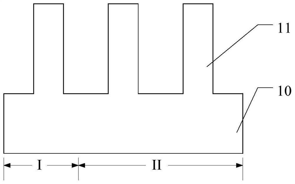
[0032] Please refer to figure 1 A substrate 10 is provided, the substrate 10 includes a first region I and a second region II, the substrate 10 has fin structures on it, and the fin structures include several fin structures 11 .

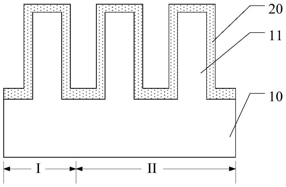
[0033] Please refer to figure 2 , forming a passivation film 20 on the surface of the fin structure and the surface of the exposed portion of the substrate 10 .

[0034] The passivation film 20 is used to repair the surface of the fin struct...


PUM


Abstract

The invention discloses a semiconductor structure and a forming method of the semiconductor structure, and the method comprises the steps: providing a substrate which is provided with a fin structure; and forming a hydrophobic film on the surface of the substrate and the surface of the fin structure. Therefore, the defects of the semiconductor structure are reduced, and the performance of the semiconductor structure is improved.

Description

technical field [0001] The invention relates to the technical field of semiconductors, in particular to a semiconductor structure and a method for forming the semiconductor structure. Background technique [0002] With the continuous development of semiconductor process technology, the process node is gradually reduced, and the gate-last process has been widely used. The HKMG (metal gate-high dielectric constant insulating layer gate structure) manufactured using the gate-last process The chip has the advantages of lower power consumption and less leakage, so that the high-frequency operation state is more stable. However, when the feature size (CD, Critical Dimension) of the device is further reduced, even if the gate-last process is adopted, the structure of the conventional metal-oxide semiconductor field-effect transistor (MOSFET) can no longer meet the requirements for device performance. Devices have received extensive attention as replacements for conventional device...

Claims


Application Information

Patent Timeline
Patent Type & Authority Applications(China)
IPC IPC(8): H01L29/78H01L29/423H01L21/336
CPCH01L29/42356H01L29/66484H01L29/7855
Inventor 张静
Owner SEMICON MFG INT (SHANGHAI) CORP
Why Eureka
Try Eureka