Supercharge Your Innovation With Domain-Expert AI Agents!

PCB defect detection method based on YOLOv5

A defect detection and defect technology, which is applied in neural learning methods, image data processing, image enhancement, etc., can solve the problems of increasing domestic enterprise costs, detection size limitations, unfavorable development, etc., and achieve excellent performance, high accuracy, The effect of high accuracy and generalization ability

Pending Publication Date: 2021-10-22
HEFEI UNIV OF TECH
View PDF0 Cites 9 Cited by
  • Summary
  • Abstract
  • Description
  • Claims
  • Application Information

AI Technical Summary

Problems solved by technology

[0003] At present, the detection of bare PCB boards mainly relies on traditional manual visual inspection, but with the continuous increase of circuit density, the difficulty of manual detection increases
In order to solve this problem, some enterprises have used the online testing method of bed of needles detection to detect it. Although this method has made significant progress compared with the traditional manual method, it also brings high cost of the template and large detection size. Restricted, the contact detection method is easy to cause damage to the bare PCB, and still cannot meet the requirements of mass production, high precision and high efficiency detection
Although the use of more advanced automatic optical inspection systems (Automatic Optical Inspection, AOI) with machine vision as the core can solve the above problems, but because most of the companies with complete functions and complete industries are foreign companies, the continuous introduction of foreign AOI equipment will undoubtedly increase the domestic market. The cost of the enterprise is not conducive to the development of the domestic industry, so solving this problem is a huge challenge for the PCB industry

Method used


Image

  • PCB defect detection method based on YOLOv5
  • PCB defect detection method based on YOLOv5
  • PCB defect detection method based on YOLOv5

Examples


Embodiment 1

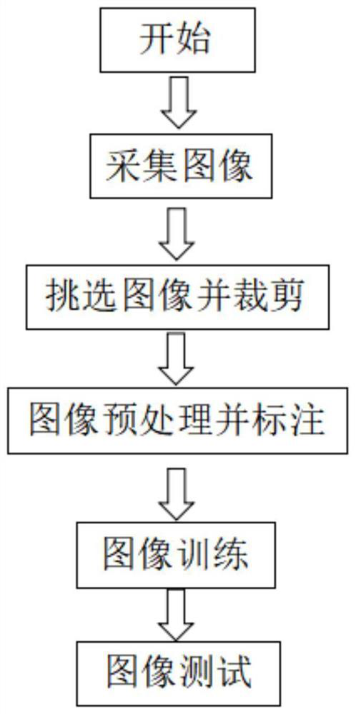
[0063] see Figure 1-11 , a PCB defect detection method based on YOLOv5, including the following steps:

[0064] Step 1. Collect images and take pictures of the produced PCB;

[0065] Step 2: Select and crop the image, select, crop and increase the brightness of the PCB image containing defects.

[0066] Step 3: Image preprocessing and labeling, use the obtained sub-images to perform data enhancement, and construct a training sample set, a verification sample set, and a test sample set;

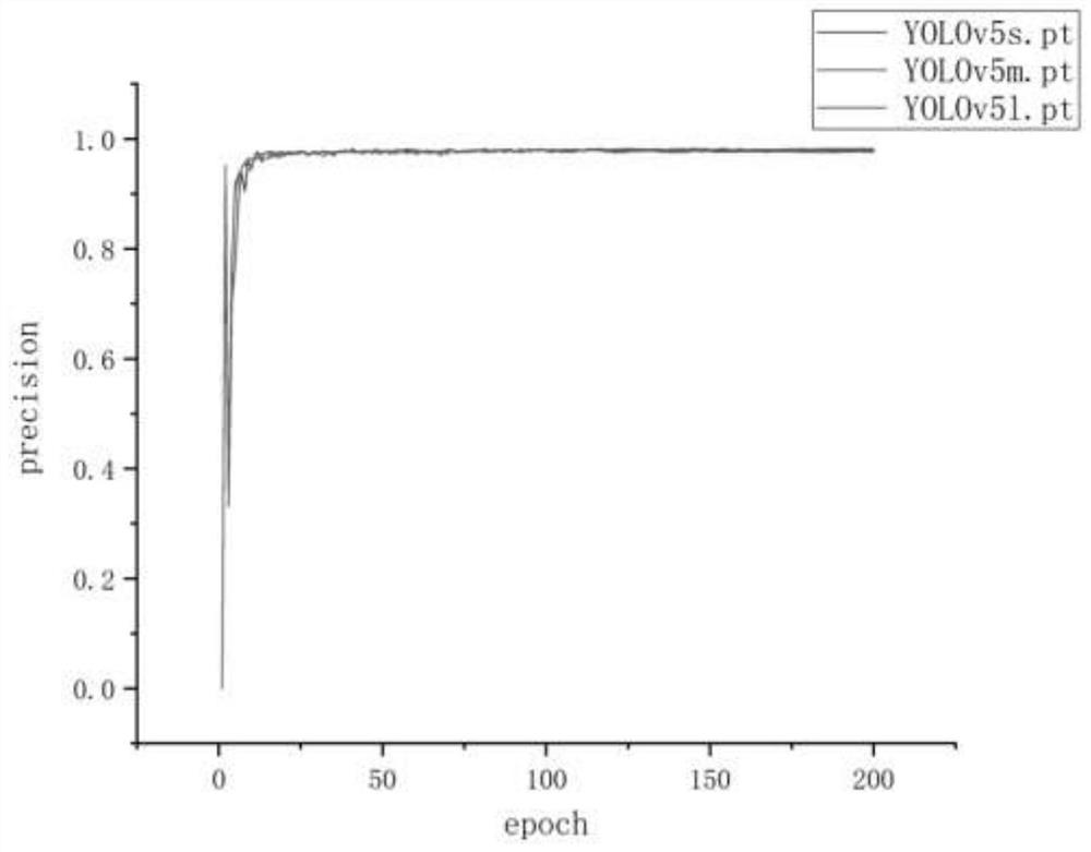
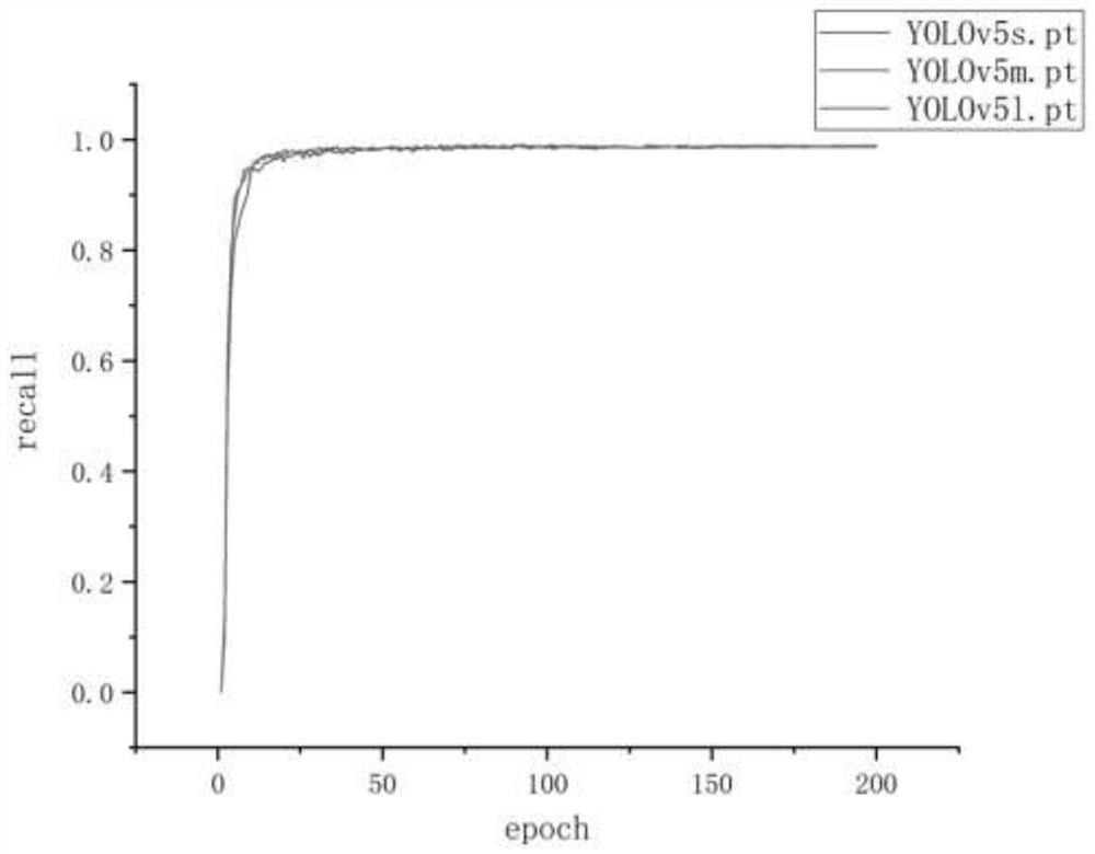
[0067] Step 4, image training, use the constructed training sample set and verification sample set to train YOLOv5 weights and verify the trained YOLOv5 model;

[0068] Step 5, image test, use the trained YOLOv5 model to detect the PCB image of the test set, and analyze the detection results.

[0069] In the embodiment of the present invention, the step 1 specifically includes the following steps:

[0070] a. Equipped with high-definition line scan cameras in the PCB production line;

[...

Embodiment 2

[0093] see figure 1 , a PCB defect detection method based on YOLOv5, including the following steps:

[0094] Step 1. Collect images and take pictures of the produced PCB;

[0095] Step 2: Select and crop the image, select, crop and increase the brightness of the PCB image containing defects.

[0096] Step 3, image preprocessing and labeling, use the obtained sub-images to perform data enhancement, and construct training sample sets, verification sample sets, and test sample sets;

[0097] Step 4, image training, use the constructed training sample set and verification sample set to train YOLOv5 weights and verify the trained YOLOv5 model;

[0098] Step 5, image test, use the trained YOLOv5 model to detect the PCB image of the test set, and analyze the detection results.

[0099] In the embodiment of the present invention, the detection method adopts the YOLOv5 target detection algorithm, which specifically includes:

[0100] 1. Mosaic data enhancement. The input end of the...


PUM


Abstract

The invention discloses a PCB defect detection method based on YOLOv5. The method comprises: image acquisition, image selection and cutting, image preprocessing and marking, image training and image testing. The method has the beneficial effects that: through testing, the accuracy rate of PCB defect detection and identification reaches 97.27%, the recall rate reaches 97.88%, the mAP (at) 0.5 value reaches 0.9877, the mAP (at) [. 5:. 95] value reaches 0.6588, and various properties are extremely excellent. Compared with the traditional image processing, the method provided by the invention has higher accuracy and generalization ability in the aspect of PCB defect surface detection. Compared with other deep learning algorithms such as Faster-RCNN for PCB surface defect detection, the method provided by the invention has higher accuracy.

Description

technical field [0001] The invention relates to a PCB defect detection method, in particular to a PCB defect detection method based on YOLOv5, and belongs to the technical field of PCB defect detection in industrial production. Background technique [0002] With the rapid development of high-tech such as big data, artificial intelligence, 5G communication, and the Internet of Things, the development of printed circuit boards (hereinafter referred to as PCB boards) has been promoted. As the mother of electronic products, the PCB board is as important to electronic products as the human heart. PCB boards are essential components of various electronic products, and the quality of electronic products depends largely on the quality of PCB boards. Therefore, PCB boards also have a great impact on the competitiveness of various brands and businesses. The quality requirements and detection efficiency requirements for PCB bare boards are also getting higher and higher. [0003] At ...

Claims


Application Information

Patent Timeline
Patent Type & Authority Applications(China)
IPC IPC(8): G06T7/00G06T7/10G06T3/40G06T3/60G06N3/04G06N3/08
CPCG06T7/0004G06T7/10G06T3/4038G06T3/4046G06T3/60G06N3/08G06T2207/20081G06T2207/20084G06T2207/20132G06T2207/30141G06N3/045
Inventor 夏远超杨永跃周博
Owner HEFEI UNIV OF TECH
Features
  • R&D
  • Intellectual Property
  • Life Sciences
  • Materials
  • Tech Scout
  • Unparalleled Data Quality
  • Higher Quality Content
  • 60% Fewer Hallucinations
Learn More