Device for detecting fatigue crack growth rate of sample in high-temperature environment
A technology of fatigue crack growth and high temperature environment, which is applied in the field of metal sample fatigue crack growth rate detection devices, can solve the problems of organic adhesive and strain sensitive components, lag of strain sensitive components, large temperature coefficient of resistance, etc., and solve the problem of poor combination problems, reduce contact resistance, and prevent high-temperature oxidation
- Summary
- Abstract
- Description
- Claims
- Application Information
AI Technical Summary
Problems solved by technology
Method used
Image
Examples
Embodiment 1
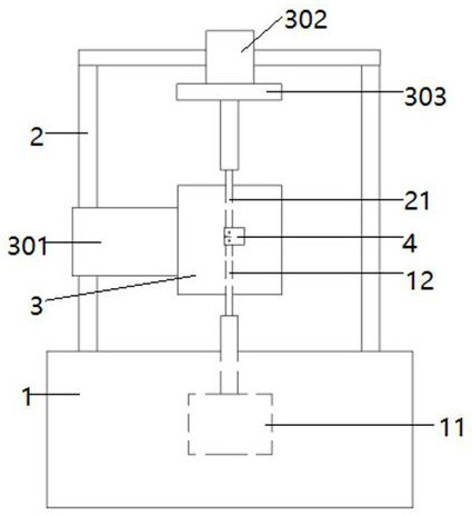
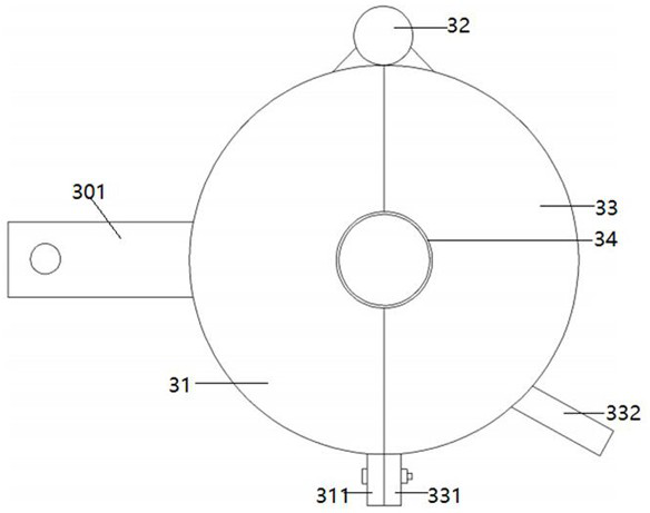
[0043] like figure 1 The embodiment shown is a high temperature environment, a sample fatigue crack spread rate detecting device, including a base 1, a frame 2 is provided on a base, a furnace 3, an upper end and a lower end opening on the rack; the rack is Up the U-shaped openings, such as figure 2 As shown, the cross section of the furnace is circular, and the furnace includes a left resonant shaft 31 that is fixedly coupled through the left fixed block 301 and the left resilient edge of the left reside, rotating with the vertical rotary axis. The left residual body and the left residual left groove and the left groove, the left groove and the right groove are provided in the left residual, and the left groove and the right groove are provided with heating wire 34. The left-resilient plate 311 on the left residual body and the right connection plate 331 provided on the right furnace body are detachably connected by bolts, and the right furnace body is provided with a handle 332;...
Embodiment 2
[0070] The thickness of the Zr film was 350 nm, the thickness of the ZrO film was 700 nm, the thickness of the AlN film was 450 nm, and the thickness of the gate NIMOMNV alloy film was 900 nm, and the thickness of the Aln protective film was 100 nm;
[0071] Among them, the elemental matching group of the NIMMNV alloy target has become Mo 9%, Mn 7%, V 6%, Ni margin; the impurity content of the NIMMNV alloy target is less than 0.01%, and the cavity defect is less than 0.05mm, the grain size is less than 30 μm. . Other content is the same as in Example 1.
Embodiment 3
[0073] The thickness of the Zr film was 350 nm, the thickness of the ZrO film was 700 nm, the thickness of the AlN film was 300 nm, and the thickness of the gate NIMOMNV alloy film was 1100 nm, and the thickness of the AlN protective film was 150 nm;
[0074] Among them, the elemental matching group of the NIMMNV alloy target became Mo 5%, Mn 5%, V 5%, Ni margin; the impurity content of NIMMNV alloy targets was less than 0.01%, and the cavity defect was less than 0.05mm, and the grain size was less than 30 μm. . Other content is the same as in Example 1.
PUM
| Property | Measurement | Unit |
|---|---|---|
| thickness | aaaaa | aaaaa |
| thickness | aaaaa | aaaaa |
| thickness | aaaaa | aaaaa |
Abstract
Description
Claims
Application Information


