Wafer performance test sample application all-in-one machine

An all-in-one spotting and all-in-one technology, applied in the field of wafer performance testing spotting all-in-one machines, can solve the problems of low wafer processing efficiency and low precision, and achieve the effect of improving equipment efficiency, improving efficiency and quality, and eliminating the problem of precision errors.

Pending Publication Date: 2021-11-02
合肥米亚科技有限公司
View PDF0 Cites 1 Cited by
  • Summary
  • Abstract
  • Description
  • Claims
  • Application Information

AI Technical Summary

Problems solved by technology

[0006] The present invention proposes an all-in-one machine for wafer performance testing and spotting, which solves the need to complete wafer spotting, drying, testing, and sample replenishment on different machines in the prior art, thus requiring repeated positioning of the wafer , which makes the wafer processing efficiency low and the precision problem

Method used


Image

  • Wafer performance test sample application all-in-one machine
  • Wafer performance test sample application all-in-one machine
  • Wafer performance test sample application all-in-one machine

Examples


Embodiment 1

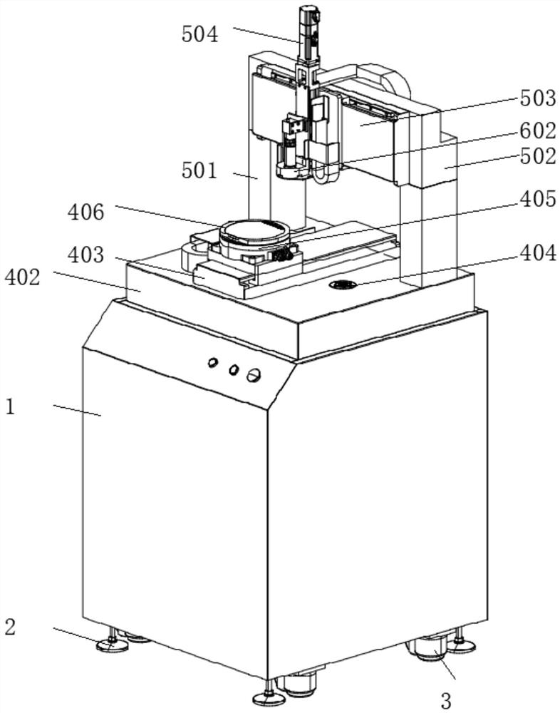
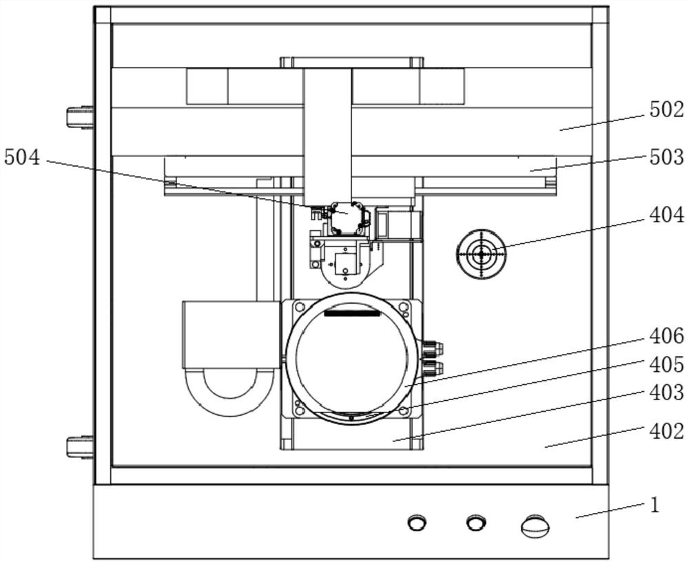
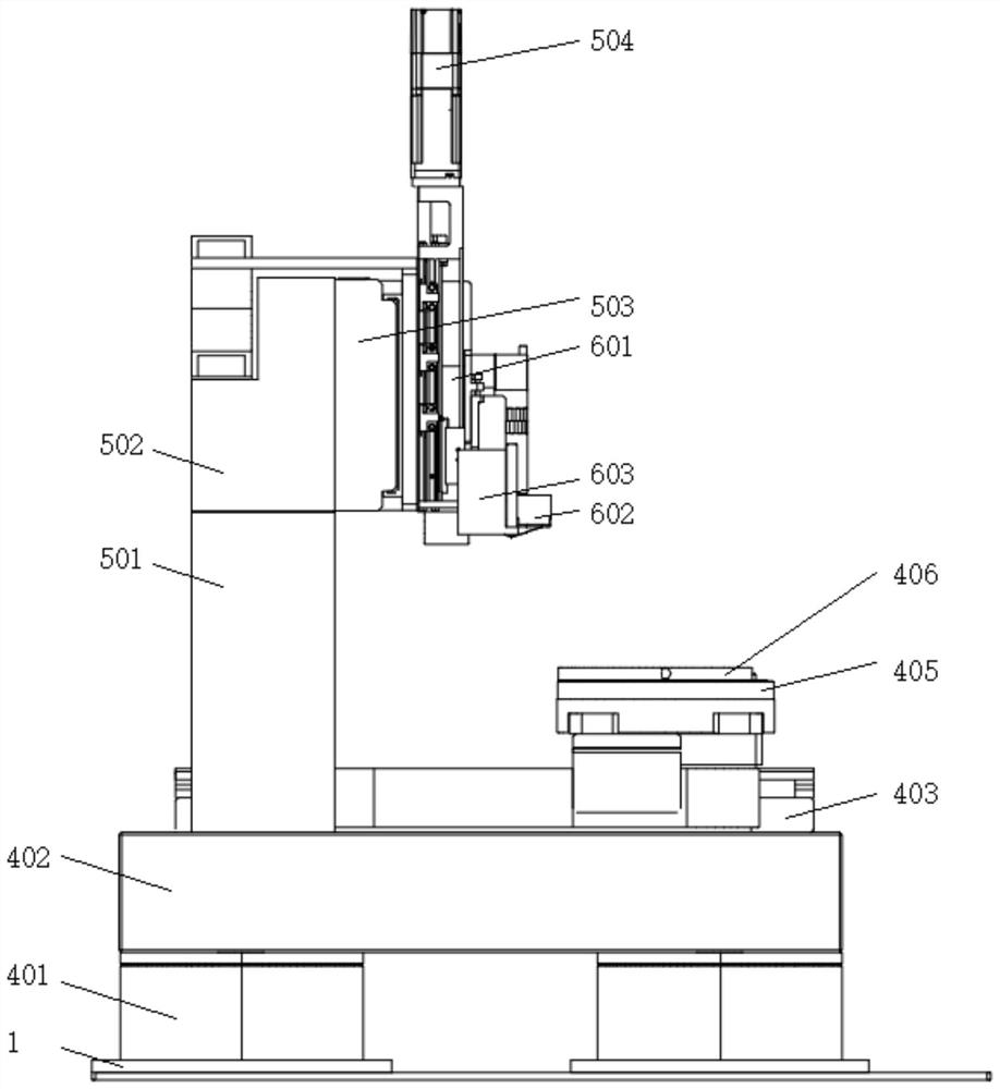
[0032] An all-in-one machine for wafer performance testing and sampling, including a system control cabinet 1, the bottom of which is symmetrically equipped with load-bearing leveling support feet 2 and universal Fuma wheel 3, and the top of the system control cabinet 1 is equipped with a wafer placement Mechanism, position adjustment mechanism and performance testing and sampling integration mechanism;

[0033] The wafer placement mechanism is arranged above the system control cabinet 1. The wafer placement mechanism is used to place the wafer when performing performance testing and spotting of the wafer. The wafer placement mechanism includes an air suspension shock absorber 401, a marble platform 402 and a Y The axis control assembly 403, the air suspension shock absorber 401 is fixed on the top of the system control cabinet 1, the marble platform 402 is arranged on the top of the air suspension shock absorber 401, and the Y axis control assembly 403 is arranged on the top o...

Embodiment 2

[0045] An all-in-one machine for wafer performance testing and sampling, including a system control cabinet 1, the bottom of which is symmetrically equipped with load-bearing leveling support feet 2 and universal Fuma wheel 3, and the top of the system control cabinet 1 is equipped with a wafer placement Mechanism, position adjustment mechanism and performance testing and sampling integration mechanism;

[0046] The system control cabinet 1 installs the control system hardware, and runs the software control system to realize the combined effect of wafer testing and spotting. By setting the universal Fuma wheel 3, any mobile device can be realized. According to the display of the universal level 404, the machine Adjust to the best balance angle to ensure the accuracy of the machine.

[0047] The wafer placement mechanism is arranged above the system control cabinet 1. The wafer placement mechanism is used to place the wafer when performing performance testing and spotting of th...


PUM


Abstract

The invention relates to the technical field of sample application and testing after wafer etching, particularly discloses a wafer performance testing and sample application all-in-one machine, and solves the problems that in the prior art, procedures such as sample application, drying, testing and sample supplementing of a wafer need to be completed on different machines, so that the wafer needs to be repeatedly positioned, and the wafer processing efficiency and precision are low. The machine comprises a system control cabinet, bearing leveling supporting legs and universal Foma wheels are symmetrically arranged at the bottom of the system control cabinet, and a wafer placing mechanism, a position adjusting mechanism and a performance testing and sample application integrated mechanism are arranged at the top of the system control cabinet; the wafer sample application and performance testing device integrates wafer sample application and performance testing, improves equipment efficiency, reduces equipment investment, realizes automatic operation of sample application and testing work, improves efficiency and quality, has sample application and performance testing functions, realizes automatic sample application according to system setting after performance testing, and improves working efficiency and wafer yield, and the cost caused by defective products is effectively reduced.

Description

technical field [0001] The invention relates to the technical field of spotting and testing after wafer etching, in particular to an all-in-one machine for wafer performance testing and spotting. Background technique [0002] Wafer generally refers to a wafer, which refers to a silicon wafer used to make silicon semiconductor circuits, and its raw material is silicon. High-purity polycrystalline silicon is dissolved and mixed with silicon crystal seeds, and then slowly pulled out to form cylindrical single crystal silicon. After the silicon ingot is ground, polished, and sliced, it forms a silicon wafer, that is, a wafer. At present, domestic wafer production lines are mainly 8-inch and 12-inch. The main processing methods of wafers are sheet processing and batch processing, that is, one or more wafers are processed at the same time. As semiconductor feature sizes become smaller and processing and measurement equipment become more advanced, new data characteristics emerge...

Claims


Application Information

Patent Timeline
Patent Type & Authority Applications(China)
IPC IPC(8): G01R31/26
Inventor 夏文君杨兴昌葛平徐建国
Owner 合肥米亚科技有限公司
Why Eureka
Try Eureka