Part, plasma reaction device and part machining method

A plasma and reaction device technology, applied in the field of plasma reaction device and parts processing, can solve the problems of failure of plasma-resistant coating protection function, peeling off, substrate corrosion damage, etc., so as to reduce the risk of peeling and prolong the transmission path, the effect of enhanced bonding

Pending Publication Date: 2021-11-02
ADVANCED MICRO FAB EQUIP INC CHINA
View PDF38 Cites 0 Cited by
  • Summary
  • Abstract
  • Description
  • Claims
  • Application Information

AI Technical Summary

Problems solved by technology

However, because the interior of the reaction chamber is a thermal cycle shock environment with constant temperature rise and fall, the thermal stress of the plasma-resistant coating coated on the surface of the substrate in the reaction chamber will continue to accumulate during service, and microcracks may occur. Even micro-cracks expand and cause cracking, peeling, etc., which makes the protective function of the plasma-resistant coating invalid, and the substrate covered by it is severely corroded due to exposure to the plasma environment in the reaction chamber.

Method used


Image

  • Part, plasma reaction device and part machining method
  • Part, plasma reaction device and part machining method
  • Part, plasma reaction device and part machining method

Examples


Embodiment Construction

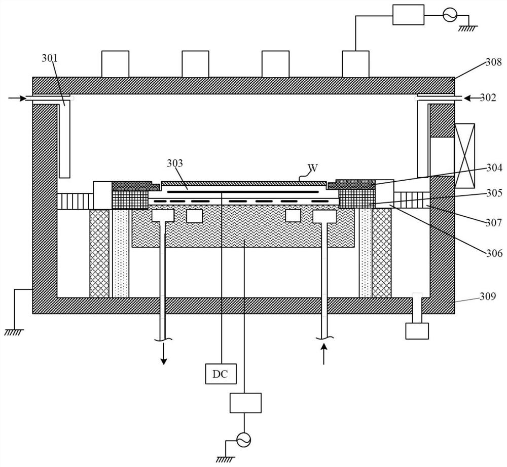
[0042] The plasma reaction device includes a reaction chamber, the reaction chamber is a plasma environment, and the parts are exposed to the plasma environment. Since the plasma is highly corrosive, it is necessary to coat the substrate surface with a corrosion-resistant coating to Prevent plasma from corroding the substrate. However, in the existing manufacturing process of semiconductor devices, the plasma-resistant coating coated on the substrate is easy to crack and peel off. The study found:

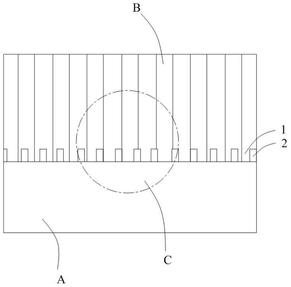
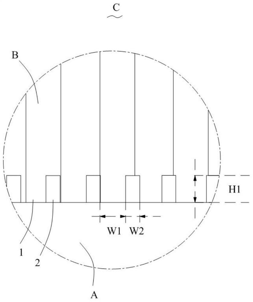
[0043] An anodized layer is arranged between the metal substrate and the plasma-resistant coating, and the anodized layer is used to realize the transition of different thermal expansion coefficients between the metal substrate and the plasma-resistant coating. Its specific manufacturing method includes firstly performing anodic oxidation treatment on the metal substrate to form a layer of anodized layer, and then coating a layer of plasma-resistant coating on the surface of the a...


PUM

PropertyMeasurementUnit
widthaaaaaaaaaa

Abstract

The invention relates to the technical field of semiconductors, in particular to a part, a plasma reaction device and a part processing method. The plasma reaction device comprises a reaction cavity, wherein the interior of the reaction cavity is a plasma environment, and the part is exposed in the plasma environment; the part comprises a substrate and a plasma-resistant coating coated on the surface of the substrate, a plurality of grooves with the width W1<=30 nm and the depth H1<=100 nm are formed in the surface of the substrate, and bulges are formed between adjacent grooves; and the plasma-resistant coating covers the side wall surfaces and the bottom surfaces of the grooves and the top surfaces of the bulges. According to the part provided by the invention, the surface of the substrate is coated with the plasma-resistant coating to carry out plasma-resistant protection on the substrate, and the plasma-resistant coating is not prone to cracking, crack propagation and stripping.

Description

technical field [0001] The invention belongs to the technical field of semiconductors, and in particular relates to a component, a plasma reaction device and a component processing method. Background technique [0002] In the manufacturing process of semiconductor devices, plasma etching is a key process for processing wafers to form design patterns. [0003] In a typical plasma etch process, the process gas (such as CF 4 , O 2 etc.) to form plasma under the action of radio frequency (Rad i oFrequency, RF) excitation. These plasmas undergo physical bombardment and chemical reactions with the wafer surface after the electric field (capacitive coupling or inductive coupling) between the upper electrode and the lower electrode, thereby etching a wafer with a specific structure. [0004] For parts in the reaction chamber, the surface is usually coated with a plasma-resistant coating to protect the substrate from plasma corrosion. However, because the interior of the reaction...

Claims


Application Information

Patent Timeline
Patent Type & Authority Applications(China)
IPC IPC(8): H01J37/32C25F3/02
CPCH01J37/32477C25F3/02H01J2237/334
Inventor 段蛟孙祥陈星建
Owner ADVANCED MICRO FAB EQUIP INC CHINA
Why Eureka
Try Eureka