Preparation method of semiconductor device

A semiconductor and device technology, applied in the field of semiconductor device preparation, can solve the problems of uneven distribution of electric field in gate trenches, poor uniformity, affecting the electrical properties of semiconductor devices, etc.

Pending Publication Date: 2021-11-02
SHANGHAI HUALI MICROELECTRONICS CORP
View PDF6 Cites 0 Cited by
  • Summary
  • Abstract
  • Description
  • Claims
  • Application Information

AI Technical Summary

Problems solved by technology

However, in the etching process of the gate trench, if the sidewall uniformity of the gate trench is poor or the bottom is not smooth enough, the electric field distribution of the gate trench will be uneven, resulting in tip discharge and white pixels. Thus affecting the electrical performance of semiconductor devices

Method used


Image

  • Preparation method of semiconductor device
  • Preparation method of semiconductor device
  • Preparation method of semiconductor device

Examples


preparation example Construction

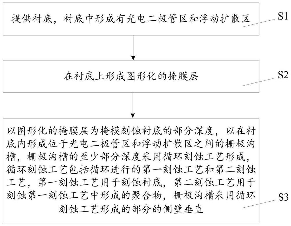
[0023] figure 1 It is a flow chart of the manufacturing method of the semiconductor device provided in this embodiment. This embodiment provides a method for manufacturing a semiconductor device, so as to reduce the generation of white pixels and improve the electrical performance of the device. Please refer to figure 1 , the preparation method of semiconductor device comprises:

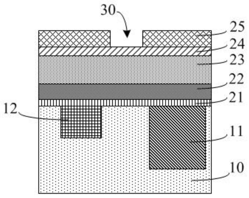
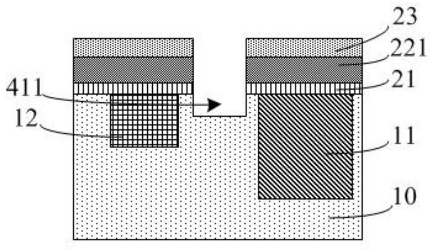
[0024] Step S1: providing a substrate in which a photodiode region and a floating diffusion region are formed;

[0025] Step S2: forming a patterned mask layer on the substrate; and,

[0026] Step S3: using the patterned mask layer as a mask to etch part of the depth of the substrate to form a gate trench between the photodiode region and the floating diffusion region in the substrate, at least part of the gate trench The depth is formed by a cyclic etching process. The cyclic etching process includes a cyclic first etching process and a second etching process. The first etching process is used t...


PUM

PropertyMeasurementUnit
Etching poweraaaaaaaaaa
Horizontal widthaaaaaaaaaa

Abstract

The invention provides a preparation method of a semiconductor device. The method comprises the steps of providing a substrate, and forming a photodiode region and a floating diffusion region in the substrate; forming a patterned mask layer on the substrate; and taking the patterned mask layer as a mask to etch partial depth of the substrate, so as to form a gate trench located between the photodiode region and the floating diffusion region in the substrate, at least partial depth of the gate trench being formed by a cyclic etching process. The circular etching process comprises a first etching process and a second etching process which are circularly carried out, the first etching process is used for etching the substrate, the second etching process is used for etching a polymer formed in the first etching process, and the side wall of the part, formed by adopting the circular etching process, of the gate trench is vertical. According to the invention, the generation of white pixels is reduced, and the electrical performance of the device is improved.

Description

technical field [0001] The invention relates to the technical field of semiconductors, in particular to a method for preparing a semiconductor device. Background technique [0002] CMOS image sensors are semiconductor devices that convert optical images into electrical signals. CMOS image sensors are widely used in mobile phone camera, industrial inspection, security and other fields. With the continuous shrinking of the pixel size in CMOS image sensors, in order to obtain better full well capacity, the ion implantation depth of the pixel area is getting deeper and deeper, which will lead to a decrease in the electron transmission efficiency in the deeper part of the photodiode, and the CMOS image sensor reads The speed is slow, which leads to image smearing and other phenomena that affect the image quality. The proposal of the vertical gate process can effectively improve the electron transmission efficiency. The vertical gate process is to change the traditional planar cha...

Claims


Application Information

Patent Timeline
IPC IPC(8): H01L21/28H01L27/146H01L29/423
CPCH01L27/14689H01L27/14614H01L29/401H01L29/4236
Inventor 董立群张磊顾珍陈彩云王奇伟
Owner SHANGHAI HUALI MICROELECTRONICS CORP
Why Eureka
Try Eureka