Circuit adhesive tape and circuit structure
A technology of circuit structure and conductive structure, applied in the directions of printed circuit, printed circuit, printed circuit manufacturing, etc., can solve the problems of complex process and low efficiency, and achieve the effect of simple process, high efficiency and reduced contact resistance.
- Summary
- Abstract
- Description
- Claims
- Application Information
AI Technical Summary
Problems solved by technology
Method used
Image
Examples
Embodiment 1
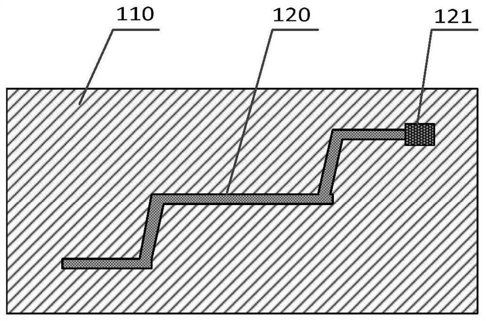
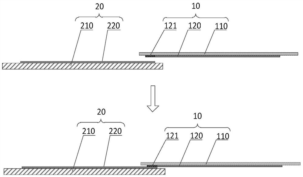
[0061] Such as figure 2 As shown, this embodiment discloses a circuit tape 10, including: a substrate 110, and a first conductive structure 120 formed on the substrate 110, the first conductive structure 120 has at least one An electrical connection portion 121 made of molten metal; wherein, the substrate 110 is made of PET, the first conductive structure 120 is made of copper foil, and the molten metal is made of gallium indium tin eutectic alloy with a melting point of 10.5°C;
[0062] When using the circuit tape, prepare a circuit board to be bonded, the circuit board has a second conductive structure, and the surface of the first conductive structure of the circuit tape is opposite to the surface of the second conductive structure of the circuit board , implementing lamination, so that the electrical connection portion of the first conductive structure overlaps the target position of the second conductive structure.
[0063] In addition, when using the circuit tape, an a...
Embodiment 2
[0065] Such as figure 2 As shown, this embodiment discloses a circuit tape, including: a substrate 110, and a first conductive structure 120 formed on the substrate 110, the first conductive structure 120 has at least one An electrical connection portion 121 formed of molten metal; wherein, the substrate 110 is selected from PI, the first conductive structure 120 is selected from a silver paste line, and the molten metal is selected from an indium-tin eutectic alloy with a melting point of 60°C;
[0066] When the circuit tape is used, it can be combined with the circuit board by means of heat pressing.
Embodiment 3
[0068] Such as Figure 5 As shown, this embodiment discloses a circuit tape, including: a substrate 110, and a first conductive structure 120 formed on the substrate 110, the first conductive structure 120 has at least one An electrical connection part 121 made of molten metal; wherein, the substrate 110 is a composite base material of PI and TPU, and the first conductive structure 120 is formed on the surface of the TPU; the surface of the TPU is also attached with a release film 130 covering the first conductive structure. The first conductive structure 120 is made of gallium-indium alloy with a melting point of 16°C.
[0069] When using this circuit tape, peel off the release film on the circuit tape, and then perform bonding with the circuit board.
PUM
| Property | Measurement | Unit |
|---|---|---|
| Melting point | aaaaa | aaaaa |
| Melting point | aaaaa | aaaaa |
Abstract
Description
Claims
Application Information
 - R&D Engineer
- R&D Manager
- IP Professional
- Industry Leading Data Capabilities
- Powerful AI technology
- Patent DNA Extraction
Browse by: Latest US Patents, China's latest patents, Technical Efficacy Thesaurus, Application Domain, Technology Topic, Popular Technical Reports.
© 2024 PatSnap. All rights reserved.Legal|Privacy policy|Modern Slavery Act Transparency Statement|Sitemap|About US| Contact US: help@patsnap.com


