Avalanche photodiode based on multi-period Bragg reflector and preparation method thereof
A technology of Bragg reflector and avalanche optoelectronics, which is applied in the field of photodetectors, can solve problems such as the influence of light absorption, difficulty in controlling the fringe electric field, and high noise, and achieve the effects of improving responsivity, improving coupling efficiency, and enhancing light absorption
- Summary
- Abstract
- Description
- Claims
- Application Information
AI Technical Summary
Problems solved by technology
Method used
Image

Examples
Embodiment 1
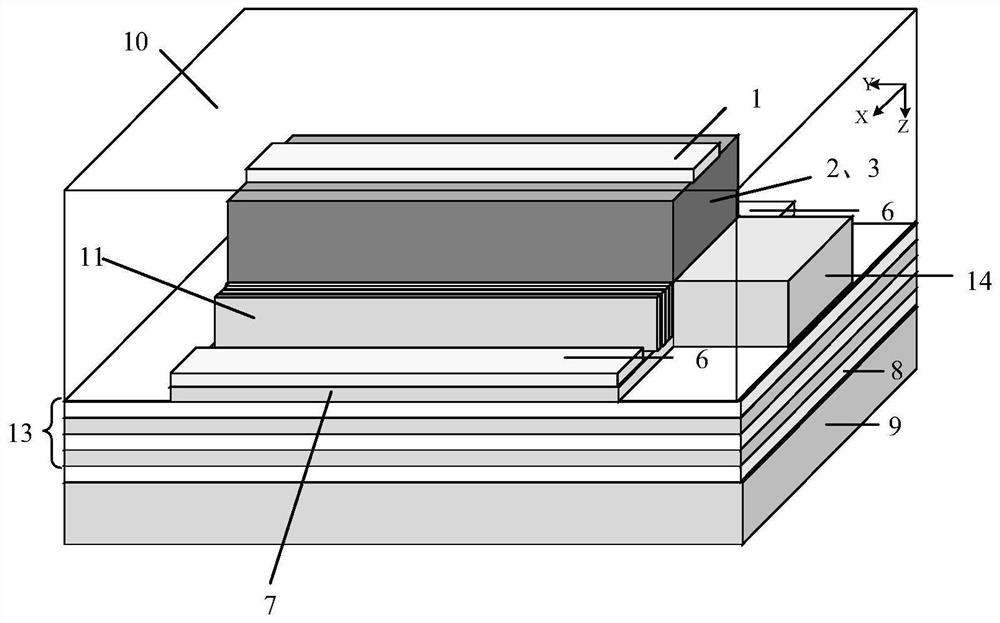
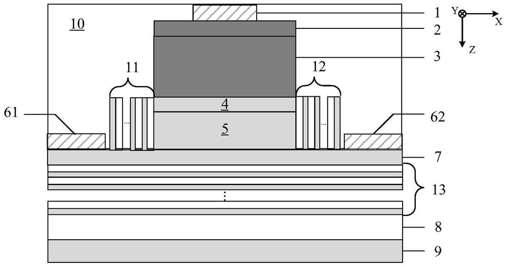
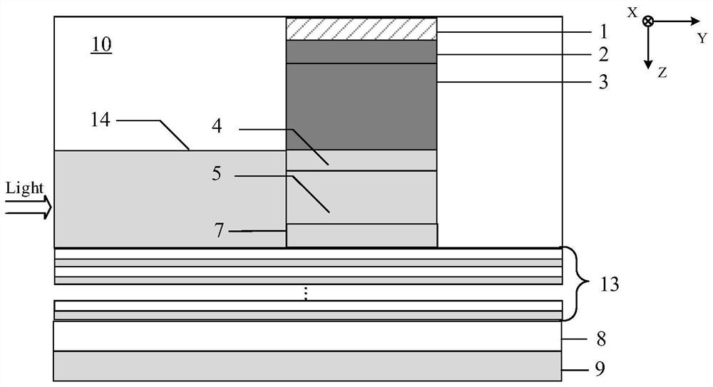
[0052] See Figure 1 to Figure 4 , figure 1 It is a schematic structural diagram of an avalanche photodiode based on a multi-period Bragg mirror provided by an embodiment of the present invention; figure 2 yes figure 1 The XZ plane cross-section of the shown multi-period Bragg mirror-based avalanche photodiode; image 3 yes figure 1 The YZ plane profile of the multiperiodic Bragg mirror-based avalanche photodiode shown; Figure 4 yes figure 1 XY plane cross-section of the shown multi-period Bragg mirror-based avalanche photodiode. The avalanche photodiode includes an anode 1, a Ge electrode contact layer 2, an absorption layer 3, a charge layer 4, a multiplication layer 5, a cathode 6, an SOI substrate, a protective layer 10, a first multi-period Bragg reflector 11, a second multi-period Bragg reflector 12 , third multi-period Bragg reflector 13 and optical waveguide 14 .
[0053] The SOI substrate sequentially includes a Si substrate 9, a SiO 2 The main function of t...
Embodiment 2
[0076] On the basis of the above embodiments, this embodiment provides a method for preparing an avalanche photodiode based on a multi-period Bragg mirror, which is used to prepare the avalanche photodiode described in the first embodiment. Such as Figure 8 Shown, the preparation method of the present embodiment comprises:
[0077] S1: Select an SOI substrate and form a third multi-period Bragg reflector on top of it, the third multi-period Bragg reflector is SiO 2 / Si laminated structure;
[0078] Specifically, the SOI substrate is selected, and the oxidation and growth of Si materials are repeated on the top of the SOI substrate to form SiO 2 A third multi-period Bragg reflector composed of / Si stacked structure, and the topmost layer of the third multi-period Bragg reflector is made of Si material.
[0079] S2: performing ion implantation on the Si material on the top of the third multi-period Bragg mirror to form a Si electrode contact layer;
[0080] Specifically, th...
PUM
| Property | Measurement | Unit |
|---|---|---|
| Thickness | aaaaa | aaaaa |
Abstract
Description
Claims
Application Information
 - Generate Ideas
- Intellectual Property
- Life Sciences
- Materials
- Tech Scout
- Unparalleled Data Quality
- Higher Quality Content
- 60% Fewer Hallucinations
Browse by: Latest US Patents, China's latest patents, Technical Efficacy Thesaurus, Application Domain, Technology Topic, Popular Technical Reports.
© 2025 PatSnap. All rights reserved.Legal|Privacy policy|Modern Slavery Act Transparency Statement|Sitemap|About US| Contact US: help@patsnap.com