
Patsnap Eureka
For R&D, Patsnap Eureka makes reading and utilizing patents & technical documents easy.
Patsnap Eureka AIR
Designed for self-driven R&D workflows. Generate viable solutions, solve complex R&D challenges, empower your innovation with AI.

Patsnap Eureka Materials
Designed for material experts only. Revolutionize your material R&D, from search, analyze, to developing new materials.

TechResearch
Generate reliable direction feasibility study reports for your R&D in just a few steps.

TechSeek
Discover and master advanced knowledge NOW. Basics, ideas, possibilities, all at once.

TechMind
As an expert in R&D Theories, TechMind can generates customized viable solutions instantly.

TechRisk
Analyze your overall solution with one click, know your potential R&D risks in advance.

TechMonitor
Get weekly tech updates, stay abreast of the latest tech innovations and key insights.
IGBT with low break-over voltage and high latch-up resistance and preparation method thereof
A high-voltage, anti-latch-up technology, applied in semiconductor/solid-state device manufacturing, circuits, electrical components, etc., can solve problems such as difficult process implementation
- Summary
- Abstract
- Description
- Claims
- Application Information
AI Technical Summary
Problems solved by technology
Method used
Image

Examples
Embodiment 1
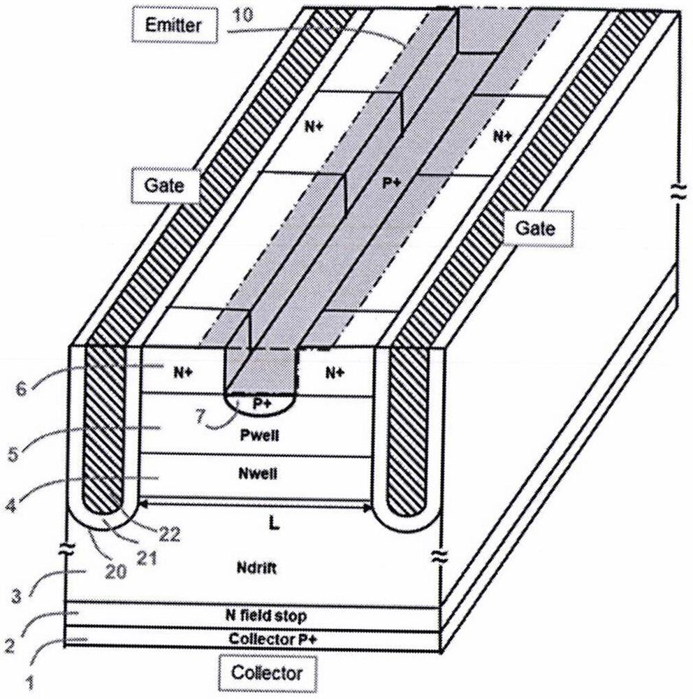
[0087] Embodiment 1 of the present invention provides an IGBT with low turn-on voltage and high latch-up resistance, which has a high-voltage terminal (collector electrode Collector), a low-voltage terminal (emitter electrode Emitter) and a control terminal (gate electrode Gate). structured as Figure 5As shown, it includes: transparent collector region 1 (Collector P+), N-type field stop layer 2 (N field stop), drift region 3 (Ndrift), where transparent collector region 1 is connected to the collector electrode; drift region 3 is located Above the transparent collector region 1 , the N-type field stop layer 2 is located between the transparent collector region 1 and the drift region 3 , and the concentration of the N-type field stop layer 2 is higher than that of the drift region 3 . The IGBT also includes a carrier storage layer 4 (Nwell), a channel body region P well 5 (Pwell), a P+ emitter region 7 (P+), an N+ emitter region 6 (N+), wherein the carrier storage layer 4 form...
Embodiment 2
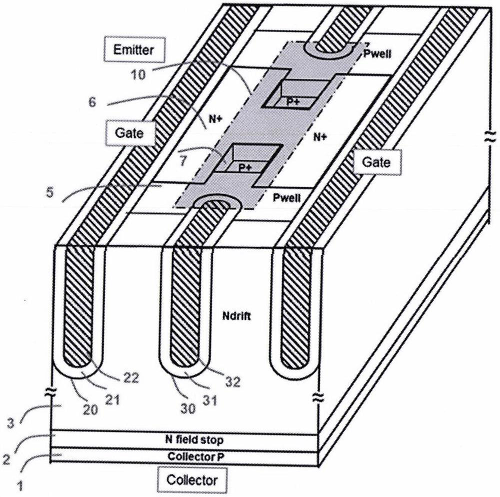
[0095] Embodiment 2 of the present invention provides an IGBT with low turn-on voltage and high latch-up resistance, such as Figure 9 shown. The IGBT has two separation trenches 30 between two trench gates 20 . Those skilled in the art will understand that the use of two separation trenches is just an example, and any number of separation trenches 30 can be added between the trench gates 20 . The advantage of this structure is that the distance between the trenches can be further reduced, and higher doping of the carrier storage layer can be used when the breakdown voltage remains unchanged. The doping concentration of the carrier storage layer is greater than 1E16cm -3 . In order to ensure the breakdown voltage, the distance between the trench 30 and the trench gate is less than 2um, ideally less than 1um, and in the two-dimensional direction, the distance between the separation trenches is less than 2um, ideally less than 1um.
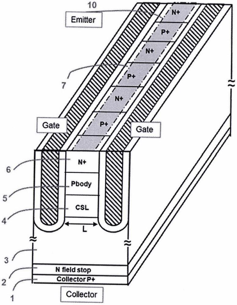
[0096] exist Figure 5 and Figure 9 In...
Embodiment 3
[0098] Embodiment 3 of the present invention provides an IGBT with low turn-on voltage and high latch-up resistance, such as Figure 10 shown. The IGBT has a trench structure 30, and the trench 30 is connected to the gate electrode.
PUM
 Abstract
Description
Claims
Application Information
 - R&D Engineer
- R&D Manager
- IP Professional
- Industry Leading Data Capabilities
- Powerful AI technology
- Patent DNA Extraction
Browse by: Latest US Patents, China's latest patents, Technical Efficacy Thesaurus, Application Domain, Technology Topic, Popular Technical Reports.
© 2024 PatSnap. All rights reserved.Legal|Privacy policy|Modern Slavery Act Transparency Statement|Sitemap|About US| Contact US: help@patsnap.com