Semiconductor structure and forming method thereof

A technology of semiconductor and dummy gate structure, which is applied in the fields of semiconductor devices, semiconductor/solid-state device manufacturing, electrical components, etc., can solve the problem that the performance of fin field effect transistors needs to be improved, and achieve the effect of high density and improved electrical performance.

Pending Publication Date: 2021-12-03
SEMICON MFG INT (SHANGHAI) CORP +1
View PDF0 Cites 2 Cited by
  • Summary
  • Abstract
  • Description
  • Claims
  • Application Information

AI Technical Summary

Problems solved by technology

[0004] However, the performance of existing fin field effect transistors needs to be improved

Method used


Image

  • Semiconductor structure and forming method thereof
  • Semiconductor structure and forming method thereof
  • Semiconductor structure and forming method thereof

Examples


Embodiment Construction

[0045] First, the reasons for the poor performance of existing semiconductor structures are described in detail in conjunction with the accompanying drawings, Figure 1 to Figure 5 It is a structural schematic diagram of each step of a method for forming a conventional semiconductor structure.

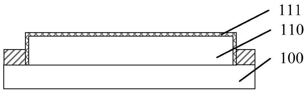
[0046] Please refer to figure 1 , providing a base 100 with a fin 110 on the base 100 and a first protective layer 111 on the surface of the fin 110 .

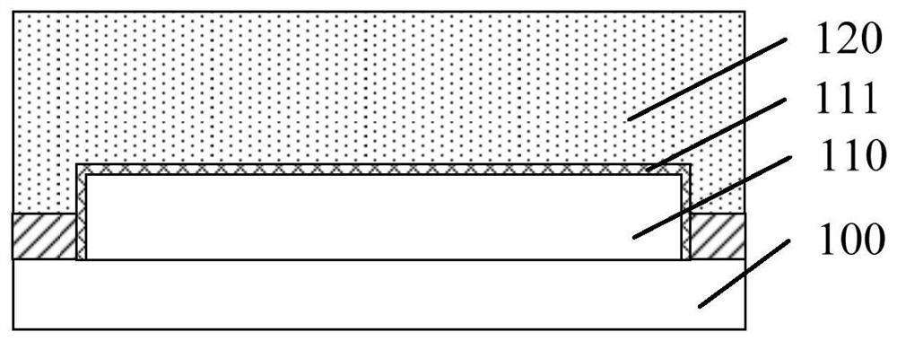
[0047] Please refer to figure 2 , forming a dummy gate material film 120 covering the top surface and the sidewall surface of the fin portion 110 on the substrate 100 .

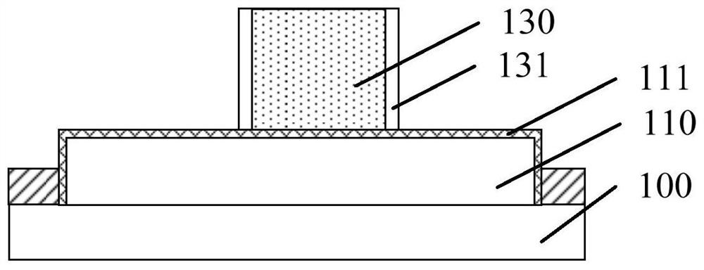
[0048] Please refer to image 3 , etching the dummy gate material film 120, forming a dummy gate structure 130 across the fin 110 on the substrate 100, and the side wall surface of the dummy gate structure 130 has a second protective layer 131 .

[0049] Please refer to Figure 4 with Figure 5 , Figure 5 yes Figure 4 In the schematic cross-sectional view al...


PUM

PropertyMeasurementUnit
thicknessaaaaaaaaaa
widthaaaaaaaaaa
widthaaaaaaaaaa

Abstract

The invention discloses a semiconductor structure and a forming method thereof, and the method comprises the steps: providing a substrate which is provided with a fin part; forming a dummy gate structure across the fin part on the substrate, wherein the surface of the side wall of the dummy gate structure is provided with a second protection layer; carrying out modification treatment on the second protective layer to enable the second protective layer to form a second modified layer; and carrying out a cleaning process. By selecting proper modification treatment, the etching rate of the second modification layer is within a preset range in the cleaning process, that is, the etching rate of the cleaning process on the second modification layer is relatively low, so that the size degree of thickness reduction of the side wall of the dummy gate structure is relatively low, the change of the included angle of a corner area at the junction of the fin part and the dummy gate structure is small, and the electrical performance of the formed semiconductor structure is improved.

Description

technical field [0001] The invention relates to the technical field of semiconductor manufacturing, in particular to a semiconductor structure and a forming method thereof. Background technique [0002] With the development of semiconductor technology, the traditional planar metal-oxide semiconductor field effect transistor is referred to as Metal-Oxide-Semiconductor Field-Effect Transistor (MOSFET). The ability to control the channel current becomes weak, causing serious leakage current. Fin Field-Effect Transistor (Fin Field-Effect Transistor) is an emerging multi-gate device, which generally includes a fin protruding from the surface of the semiconductor substrate, and a gate structure covering part of the top surface and sidewall of the fin. , source and drain doped regions in the fins on both sides of the gate structure. [0003] The forming method of the gate structure is: forming a gate material film covering the fins on the substrate; forming a patterned layer on t...

Claims


Application Information

Patent Timeline
Patent Type & Authority Applications(China)
IPC IPC(8): H01L21/336H01L29/78H01L21/28
CPCH01L29/66803H01L29/66545H01L29/785H01L21/28141
Inventor 王艳良
Owner SEMICON MFG INT (SHANGHAI) CORP
Why Eureka
Try Eureka