Metamaterial wave-absorbing structure applied to millimeter wave radar, and vehicle antenna thereof
A technology of millimeter-wave radar and metamaterials, which is applied to antennas, antennas, and antenna parts suitable for movable objects. The number of layers of splitting structure is too many to achieve good absorbing effect, good absorbing performance and reduce multipath effect
- Summary
- Abstract
- Description
- Claims
- Application Information
AI Technical Summary
Problems solved by technology
Method used
Image
Examples
Embodiment 1
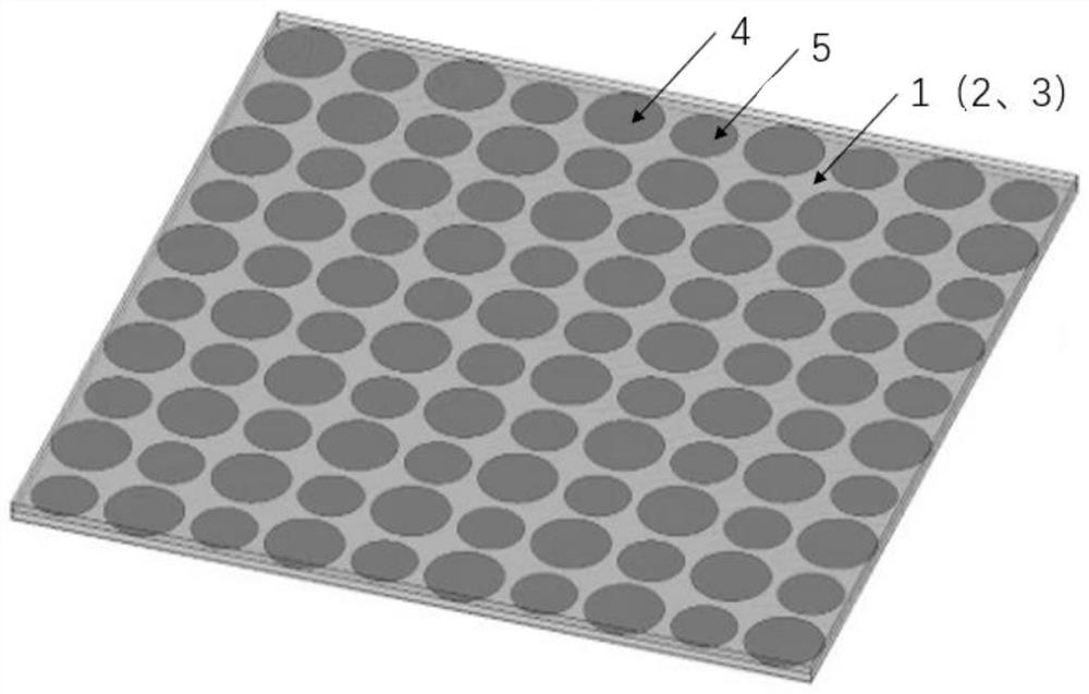
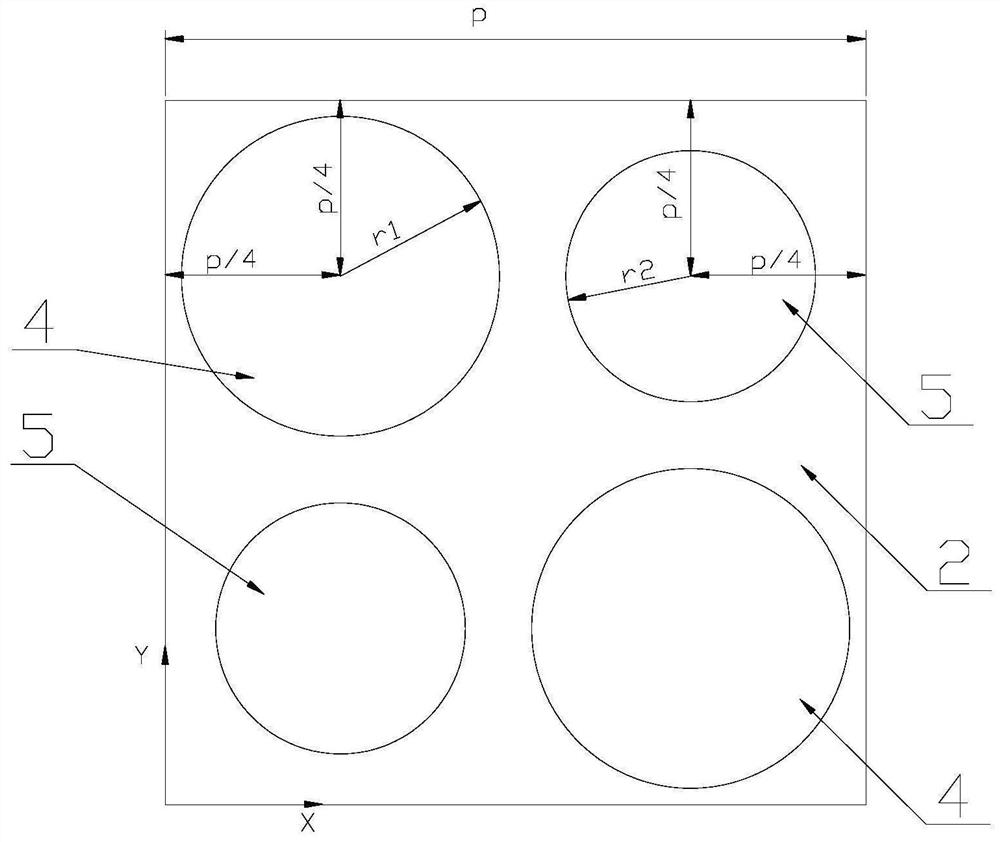
[0031] Such as Figure 1-3 As shown, the present invention provides a metamaterial wave-absorbing structure applied to millimeter-wave radar, which includes a plurality of square wave-absorbing units arranged periodically and closely in the horizontal direction. The metal reflective layer 1, the first dielectric layer 2, the supersurface layer, and the second dielectric layer 3 are placed, and the metal reflective layer 1, the first dielectric layer 2, and the second dielectric layer 3 are all square sheets with a side length of p, Edges of the metal reflective layer 1 , the first dielectric layer 2 , and the second dielectric layer 3 are vertically aligned.
[0032] The supersurface layer comprises two large circular wave-absorbing sheets 4 and two small circular wave-absorbing sheets 5, and the two large circular wave-absorbing sheets 4 are arranged at a pair of corners on the first dielectric layer 2 ( figure 2 middle upper left corner and lower right corner), two small c...
Embodiment 2
[0037] In this embodiment, except for the following features, the absorbing structure is exactly the same as that of Embodiment 1:
[0038] The material of the metal reflection layer 1 is copper, and the thickness of the metal reflection layer 1 is t=0.015mm. Both the first dielectric layer 2 and the second dielectric layer 3 are made of polyvinyl fluoride, and both have a dielectric constant of 2.3. The thickness h1 of the first dielectric layer 2 and the thickness h2 of the second dielectric layer 3 are the same, h1=h2=1.0mm. The side length p is 20 mm, the radius r1 of the large circular wave-absorbing sheet 4 = 4.7 mm, and the radius r2 of the small circular wave-absorbing sheet 5 = 3.9 mm. The material of the supersurface layer is indium tin oxide, and the square resistance of the supersurface layer is 110Ω / m 2 . When multiple absorbing units are arranged horizontally and periodically, they are closely arranged along the X-axis direction and the Y-axis direction to for...
Embodiment 3
[0041] In this embodiment, except for the following features, the absorbing structure is exactly the same as that of the embodiment:
[0042] The material of the metal reflection layer 1 is copper, and the thickness of the metal reflection layer 1 is t=0.018mm. Both the first dielectric layer 2 and the second dielectric layer 3 are made of polylactic acid, and the dielectric constants are both 2.2. The thickness h1 of the first dielectric layer 2 and the thickness h2 of the second dielectric layer 3 are the same, h1=h2=0.8mm. The side length p is 19.8mm, the radius r1 of the large circular absorbing sheet 4 is 4.8mm, and the radius of the small circular absorbing sheet 5 is r2=4.2mm. The material of the supersurface layer is indium tin oxide, and the square resistance of the supersurface layer is 90Ω / m 2 . When multiple absorbing units are arranged horizontally and periodically, they are closely arranged along the X-axis direction and the Y-axis direction to form a matrix. ...
PUM
 Abstract
Description
Claims
Application Information
 - R&D
- Intellectual Property
- Life Sciences
- Materials
- Tech Scout
- Unparalleled Data Quality
- Higher Quality Content
- 60% Fewer Hallucinations
Browse by: Latest US Patents, China's latest patents, Technical Efficacy Thesaurus, Application Domain, Technology Topic, Popular Technical Reports.
© 2025 PatSnap. All rights reserved.Legal|Privacy policy|Modern Slavery Act Transparency Statement|Sitemap|About US| Contact US: help@patsnap.com


