Invisible semiconductor device and preparation method and application thereof

A semi-conductor and invisible technology, which is applied in the manufacture of semiconductor devices, electrical components, final products, etc., can solve the problems of damage to the uniformity of nano-column crystal quality, difficulty in guaranteeing the quality of epitaxial crystals, easy damage to graphene or nano-columns, etc., to achieve effective Facilitate reuse, controllable cost and long service life

Pending Publication Date: 2021-12-10
SUZHOU INST OF NANO TECH & NANO BIONICS CHINESE ACEDEMY OF SCI +1
View PDF0 Cites 1 Cited by
  • Summary
  • Abstract
  • Description
  • Claims
  • Application Information

AI Technical Summary

Problems solved by technology

At present, it has been reported (CN107785355A, Adv.Mater.2011, 23, 4614) that the SiO 2 /Si surface to prepare graphene, re-grow GaN-based nanocolumn arrays (i.e. one-dimensional GaN-based materials), and finally peel graphene and nanocolumns and transfer them to flexible substrates; this scheme can theoretically prepare flexible devices with transparency , but there are certain limitations: A. It is not yet mature to directly grow one-dimensional GaN-based materials directly on graphene, and the quality of its epitaxial crystals is difficult to guarantee. During the epitaxial growth process, graphene will also be destroyed to a certain extent Damage; B. Graphene itself is an extremely thin film, the thickness of a single layer of graphene is about 0.1nm, and graphene itself is extremely easy to be

Method used


Image

  • Invisible semiconductor device and preparation method and application thereof
  • Invisible semiconductor device and preparation method and application thereof
  • Invisible semiconductor device and preparation method and application thereof

Examples


preparation example Construction

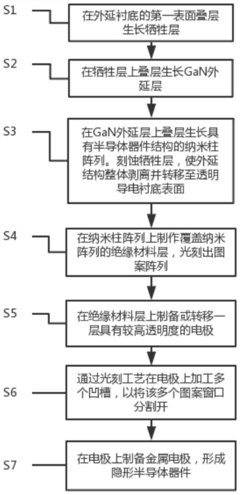
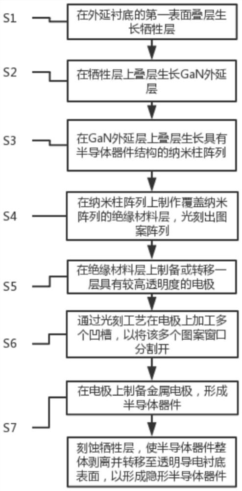
[0093] see figure 1 , an embodiment of the present invention provides a method for manufacturing a stealth semiconductor device, which includes:

[0094] S1. A sacrificial layer is stacked and grown on the first surface of the epitaxial substrate, and the total thickness of the sacrificial layer is H 0 , 1nm≤H 0 <100nm;

[0095] S2, stacking and growing a GaN epitaxial layer with pores or defects on the sacrificial layer, with a total thickness of H 1 , 1nm≤H 1 <600nm;

[0096] S3. On the GaN epitaxial layer, grow a nanocolumn array with a semiconductor device structure; prepare an etching electrode on the second surface of the epitaxial substrate opposite to the first surface, and make the etching electrode and the sacrificial electrode The layers are turned on, and then the sacrificial layer is removed by electrochemical etching, so as to peel off the epitaxial structure above the sacrificial layer as a whole, and transfer it to the surface of the transparent conductive...

Embodiment 1

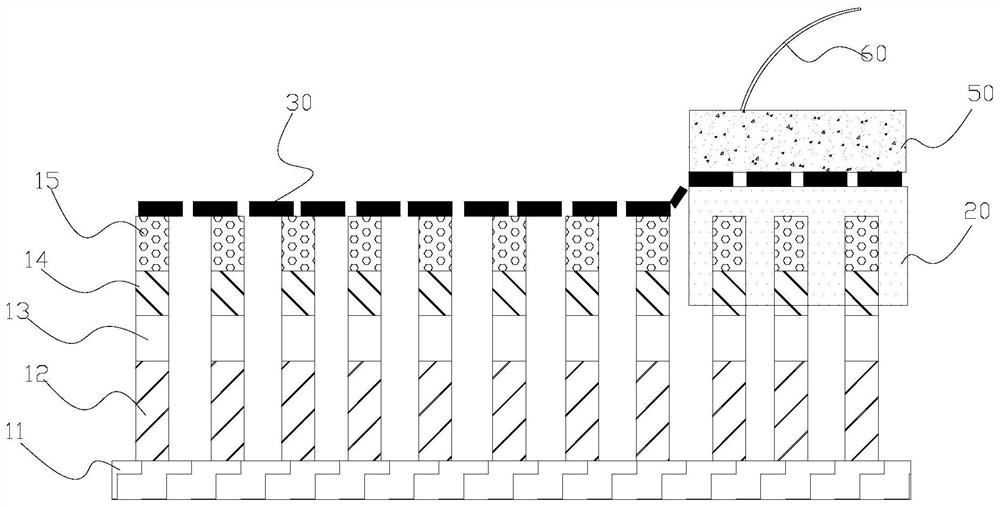
[0122] 1) First, place the silicon substrate in a molecular beam epitaxy (MBE) growth chamber for epitaxial growth, see Figure 4 , including the following steps:

[0123] In the first step, an AlN sacrificial layer 10 with a thickness of about 5 nm is grown on the front side of the n-type doped silicon (Si) substrate;

[0124] The second step is to grow a Si-doped GaN epitaxial layer 11 with a thickness of 20 nm and a thickness of 20 nm on the AlN sacrificial layer 10, and the doping concentration is 1×10 22 cm -3 ;

[0125] In the third step, a layer of Si-doped GaN nanocolumns 12 with a height of about 500 nm is grown on the GaN epitaxial layer 11, and the doping concentration is 1×10 22 cm -3 ;

[0126] The fourth step is to grow a layer of In with a thickness of 50nm on the GaN nanocolumn 12 0.3 Ga 0.7 N nanopillars13.

[0127] The fifth step, in the In 0.3 Ga 0.7 A layer of Al with a thickness of 10 nm is grown on the N nanopillar 13 0.2 Ga 0.8 N nanocolumns ...

Embodiment 2

[0137] This embodiment is basically the same as Embodiment 1, the difference is that In in this embodiment 1-n-x Al n Ga x There are 6 In in the N nanopillar 0.25 Ga 0.75 The superlattice-like structure of N(15nm) / GaN(5nm), that is, In 0.25 Ga 0.75 N (15nm) and GaN (5nm) are arranged alternately, with a total of 6 periods, in which the values ​​of x in two adjacent layers are 0.75 and 1 respectively, and the values ​​of n are both 0. In addition, there is a layer of hydrogel about 1 μm thick on the surface of the transferred transparent conductive substrate, which is used to fix the nanocolumns, and the device can be used as a light-emitting device.


PUM

PropertyMeasurementUnit
Heightaaaaaaaaaa
Heightaaaaaaaaaa
Heightaaaaaaaaaa

Abstract

The invention discloses an invisible semiconductor device and a preparation method and application thereof. The preparation method comprises the steps of sequentially forming a sacrificial layer, an epitaxial layer and a nano-pillar array on an epitaxial substrate, wherein the epitaxial layer and the nano-pillar array both contain III-V group semiconductor materials; arranging an insulating material layer which at least covers the nano-pillar array, and processing at least one window on the insulating material layer so as to enable at least part of the nano-pillar array to be exposed from the window; and arranging a first electrode at the window of the insulating material layer, and enabling the first electrode to be electrically connected with the nano-pillar array exposed out of the window, wherein the first electrode is a transparent electrode, a second electrode is arranged on the area, which is except the window, of the insulating material layer, and then the invisible semiconductor device is formed. The invisible semiconductor device provided by the invention is long in service life, and the invisible semiconductor device is provided with the vertical nanorod array, thereby facilitating the release of epitaxial stress and improving the crystal quality.

Description

technical field [0001] The invention relates to a stealth semiconductor device, in particular to a stealth semiconductor device and its preparation method and application, belonging to the technical field of semiconductor devices. Background technique [0002] Invisible, commonly known as "invisible", and "transparent" can also achieve the effect of invisibility. In recent years, stealth technology has received more and more attention from all over the world. It can be applied to stealth aircraft, invisibility cloaks, etc. It is a high-tech technology that human beings dream of. In order to achieve invisibility, many researchers have introduced negative refractive index materials, hoping to achieve "transparency" through complex electromagnetic wave regulation. Although the application of this technology has broad prospects, it is extremely difficult and it will still take a long time for the real application. Therefore, stealth technology will remain a worldwide difficult...

Claims


Application Information

Patent Timeline
IPC IPC(8): H01L33/00H01L33/22H01L33/42H01L31/18H01L31/0236H01L31/0224B82Y40/00B82Y10/00
CPCH01L33/0062H01L33/42H01L33/005H01L33/22H01L31/18H01L31/1848H01L31/02366H01L31/022408H01L31/022466B82Y10/00B82Y40/00H01L2933/0016Y02P70/50
Inventor 张建亚陆书龙赵宇坤邢志伟周敏
Owner SUZHOU INST OF NANO TECH & NANO BIONICS CHINESE ACEDEMY OF SCI
Why Eureka
Try Eureka