Silicon-based active matrix type organic light-emitting display and manufacturing method thereof
A technology of a light-emitting display and a manufacturing method, applied in the field of OLED displays, can solve the problems that fine metal masks cannot achieve good alignment, pixel electrical crosstalk, and high device resolution, so as to avoid display defects, reduce electrical crosstalk, and achieve high color. domain effect
- Summary
- Abstract
- Description
- Claims
- Application Information
AI Technical Summary
Problems solved by technology
Method used
Image


Examples
Embodiment 1
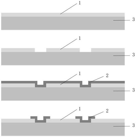
[0038] This embodiment specifically discloses a method for manufacturing a silicon-based active matrix organic light-emitting display, which specifically includes the following steps:
[0039] First, Al is prepared on the substrate 3 as the highly reflective anode metal layer 1, and the fabrication methods include physical vapor deposition and electron beam evaporation;
[0040] Second, perform photolithography and etching patterning on the highly reflective anode metal layer 1 to form an anode pixel structure, and perform deglue treatment on the highly reflective anode metal layer 1 by a dry method or a wet method;
[0041] Third, grow a pixel isolation layer 2 on a substrate 3 with an anode pixel structure, and the material of the isolation layer is SiO x or SiN x ;
[0042] Fourth, the pixel isolation layer 2 is patterned by photolithography to form an array structure;
[0043] Fifth, the pixel isolation layer 2 is etched. After etching, the pixel isolation layer covers ...
Embodiment 2
[0046] This embodiment specifically discloses a method for manufacturing a silicon-based active matrix organic light-emitting display, which specifically includes the following steps:
[0047] (1) On the silicon-based (or glass) substrate 3, use the method of sputtering metal deposition in physical vapor deposition to deposit and prepare a highly reflective anode metal layer Al, and the thickness of the Al layer is 50nm~300nm;
[0048] (2) On the highly reflective anode metal layer Al, spin-coat i-line photoresist, perform exposure and development processes, and realize the required anode electrode pattern on the photoresist;
[0049] (3) Then use methods such as dry etching to etch the metal film, that is, the highly reflective anode metal layer Al, and finally remove the photoresist to realize the patterning of the metal film;
[0050] (4) After step (3) is completed, a layer of SiN is deposited on the highly reflective anode metal layer by chemical vapor deposition. x or S...
PUM
| Property | Measurement | Unit |
|---|---|---|
| Thickness | aaaaa | aaaaa |
| Thickness | aaaaa | aaaaa |
Abstract
Description
Claims
Application Information
 - R&D
- Intellectual Property
- Life Sciences
- Materials
- Tech Scout
- Unparalleled Data Quality
- Higher Quality Content
- 60% Fewer Hallucinations
Browse by: Latest US Patents, China's latest patents, Technical Efficacy Thesaurus, Application Domain, Technology Topic, Popular Technical Reports.
© 2025 PatSnap. All rights reserved.Legal|Privacy policy|Modern Slavery Act Transparency Statement|Sitemap|About US| Contact US: help@patsnap.com