Semiconductor epitaxial structure and application thereof

An epitaxial structure and semiconductor technology, which is applied in the direction of semiconductor devices, semiconductor/solid-state device manufacturing, electrical components, etc., can solve the problems of affecting ion doping efficiency, affecting chip luminous efficiency, and low electrostatic capacity, so as to increase the number of photons, Effect of improving surface morphology and improving quality

Pending Publication Date: 2021-12-17
SHENZHEN JING XIANG TECH CO LTD +2
View PDF0 Cites 0 Cited by
  • Summary
  • Abstract
  • Description
  • Claims
  • Application Information

AI Technical Summary

Problems solved by technology

The positive and negative electrodes of the diode chip on the sapphire substrate are located on the same side of the chip, and the spacing is very small, so the ability to withstand static electricity is very small, and it is very easy to be broken down by static electricity, which affects the life of the device
[0003] GaN / InGaN quantum well barrier regions are used in the active region of the semiconductor epitaxial structure of gallium nitride-based diodes, but due to the difference in lattice constants of GaN / AlGaN two materials, it is easy to produce polarization effects and cause dislocation defects. Defects cannot be effectively controlled, and the line dislocations passing through the GaN / InGaN quantum well barrier region will cause a large number of surface defects and form leakage channels. Surface defects also affect the efficiency of ion doping in the semiconductor layer on both sides of the light-emitting layer, thereby affecting Affect the hole concentration and affect the luminous efficiency of the chip

Method used


Image

  • Semiconductor epitaxial structure and application thereof
  • Semiconductor epitaxial structure and application thereof
  • Semiconductor epitaxial structure and application thereof

Examples


Embodiment Construction

[0070] Embodiments of the present invention are described below through specific examples, and those skilled in the art can easily understand other advantages and effects of the present invention from the content disclosed in this specification. The present invention can also be implemented or applied through other different specific implementation modes, and various modifications or changes can be made to the details in this specification based on different viewpoints and applications without departing from the spirit of the present invention.

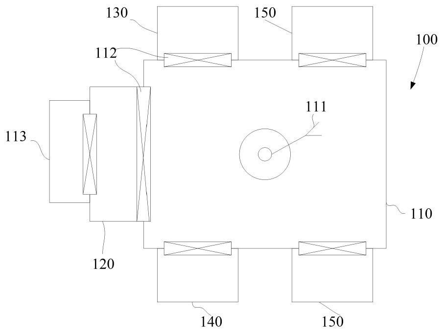
[0071] see figure 1 , this embodiment proposes a semiconductor device 100, which may be, for example, a chemical vapor deposition device, or a physical vapor deposition device, or a combination of physical vapor deposition device, chemical vapor deposition device, or other semiconductor devices.

[0072] Such as figure 1 As shown, in one embodiment of the present invention, a plurality of chambers are provided in the semiconductor de...


PUM

PropertyMeasurementUnit
thicknessaaaaaaaaaa
thicknessaaaaaaaaaa
thicknessaaaaaaaaaa

Abstract

The invention provides a semiconductor epitaxial structure and application thereof. The structure comprises: a substrate. a first semiconductor layer arranged on the substrate; an active layer arranged on the first semiconductor layer; a second semiconductor layer arranged on the active layer; and a hole injection layer arranged on the second semiconductor layer, wherein the hole injection layer comprises a non-or low-doped gallium nitride layer and/or a doped gallium nitride layer. According to the semiconductor epitaxial structure provided by the invention, the quality of the semiconductor epitaxial structure can be improved.

Description

technical field [0001] The invention relates to the field of semiconductors, in particular to a semiconductor epitaxial structure and its application. Background technique [0002] Gallium nitride (GaN) is a wide bandgap material with high resistivity. The electrostatic charges generated during the production and transportation of GaN-based diode chips are not easy to disappear, and can generate high electrostatic voltage when accumulated to a certain extent. The positive and negative electrodes of the diode chip on the sapphire substrate are located on the same side of the chip, and the spacing is very small, so the ability to withstand static electricity is very small, and it is very easy to be broken down by static electricity, which affects the life of the device. [0003] GaN / InGaN quantum well barrier regions are used in the active region of the semiconductor epitaxial structure of gallium nitride-based diodes, but due to the difference in lattice constants of GaN / AlGa...

Claims


Application Information

Patent Timeline
Patent Type & Authority Applications(China)
IPC IPC(8): H01L21/677H01L21/67H01L33/00
CPCH01L21/67781H01L21/67092H01L33/005
Inventor 陈卫军
Owner SHENZHEN JING XIANG TECH CO LTD
Why Eureka
Try Eureka