
Eureka
For R&D, Eureka makes reading and utilizing patents & technical documents easy.
Eureka AIR
Designed for self-driven R&D workflows. Generate viable solutions, solve complex R&D challenges, empower your innovation with AI.

Eureka Materials
Designed for material experts only. Revolutionize your material R&D, from search, analyze, to developing new materials.

TechResearch
Generate reliable direction feasibility study reports for your R&D in just a few steps.

TechSeek
Discover and master advanced knowledge NOW. Basics, ideas, possibilities, all at once.

TechMind
As an expert in R&D Theories, TechMind can generates customized viable solutions instantly.

TechRisk
Analyze your overall solution with one click, know your potential R&D risks in advance.

TechMonitor
Get weekly tech updates, stay abreast of the latest tech innovations and key insights.
Semiconductor epitaxial wafer, preparation method thereof and microwave communication transistor
A technology of semiconductors and epitaxial wafers, which is applied in semiconductor/solid-state device manufacturing, circuits, electrical components, etc., can solve the problems of microwave communication transistor leakage current and component reliability, and achieve improved leakage current, good device stability and reproducible effect
- Summary
- Abstract
- Description
- Claims
- Application Information
AI Technical Summary
Problems solved by technology
Method used
Image

Examples
preparation example Construction
[0054] The present application also provides a method for preparing a semiconductor epitaxial wafer, comprising:
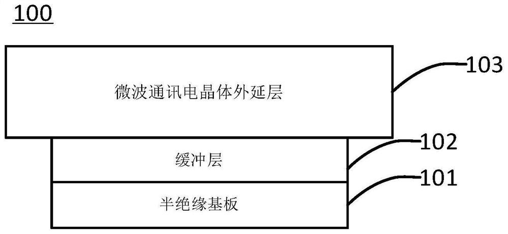
[0055] A substrate and a reaction chamber are provided, and the substrate is a semi-insulating compound semiconductor substrate. In this step, the selection of the substrate may be the same as the selection of the structure of the above-mentioned semiconductor epitaxial wafer, which will not be repeated here.
[0056] A reaction gas containing oxygen atoms is introduced into the reaction chamber.
[0057] In the case of continuously feeding the reaction gas containing oxygen atoms, the epitaxial growth of the semiconductor layer is carried out by means of organometallic vapor deposition.
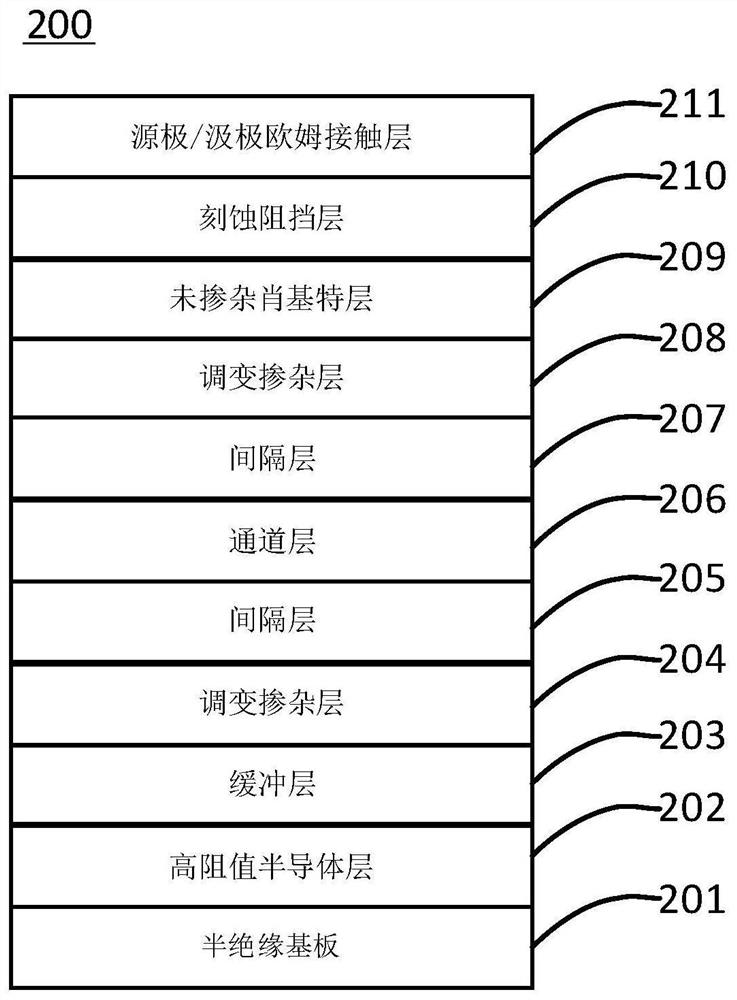
[0058] In this embodiment, a method for preparing a semiconductor epitaxial wafer is provided. The semiconductor epitaxial wafer including the substrate and the semiconductor layer is prepared by using the semiconductor epitaxial wafer preparation method. The semiconductor ep...
PUM
| Property | Measurement | Unit |
|---|---|---|
| thickness | aaaaa | aaaaa |
| thickness | aaaaa | aaaaa |
| thickness | aaaaa | aaaaa |
Abstract
Description
Claims
Application Information
 - R&D Engineer
- R&D Manager
- IP Professional
- Industry Leading Data Capabilities
- Powerful AI technology
- Patent DNA Extraction
Browse by: Latest US Patents, China's latest patents, Technical Efficacy Thesaurus, Application Domain, Technology Topic, Popular Technical Reports.
© 2024 PatSnap. All rights reserved.Legal|Privacy policy|Modern Slavery Act Transparency Statement|Sitemap|About US| Contact US: help@patsnap.com