
Forming method of CMOS image sensor

An image sensor and semiconductor technology, applied in the fields of electrical solid state devices, semiconductor devices, semiconductor/solid state device manufacturing, etc., can solve problems affecting product yield and image quality, white pixels, dark current, etc., and reduce plasma-induced damage. , the effect of improving the signal-to-noise ratio and improving the performance

Pending Publication Date: 2021-12-21
GALAXYCORE SHANGHAI
View PDF0 Cites 0 Cited by
  • Summary
  • Abstract
  • Description
  • Claims
  • Application Information

AI Technical Summary

Problems solved by technology

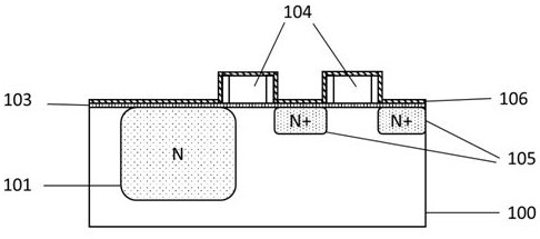
[0004] However, during the formation of the self-aligned silicide barrier layer or in the subsequent process, plasma is often introduced to bring plasma-induced damage (Plasma Induced Damage, PID), resulting in the formation of a large number of dangling bonds on the silicon-oxygen surface. The existence of the key is easy to generate electrons in the dark field of the image sensor, and these electrons are collected by the photodiode, resulting in dark current or white pixel (White Pixel, WP) phenomenon, affecting product yield and image quality

Method used


Image

  • Forming method of CMOS image sensor
  • Forming method of CMOS image sensor
  • Forming method of CMOS image sensor

Examples


Embodiment Construction

[0021] In order to solve the above-mentioned problems in the prior art, the present invention provides a method for forming a CMOS image sensor, which reduces the plasma-induced damage caused by subsequent processes, reduces the generation of dark current and white pixels, improves the signal-to-noise ratio of CIS, and improves Product yield and image quality, improving image sensor performance.

[0022] In the following detailed description of the preferred embodiment, reference is made to the accompanying drawings which form a part hereof. The accompanying drawings show, by way of example, specific embodiments in which the invention can be practiced. The illustrated embodiments are not intended to be exhaustive of all embodiments in accordance with the invention. It is to be understood that other embodiments may be utilized and structural or logical changes may be made without departing from the scope of the present invention. Accordingly, the following detailed descriptio...


PUM

PropertyMeasurementUnit
thicknessaaaaaaaaaa

Abstract

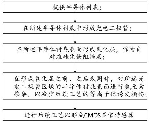
According to a forming method of a CMOS image sensor provided by the invention, nitrogen element doping is carried out on the surface of a semiconductor substrate in a photodiode region, and the doped nitrogen element can form a silicon-nitrogen bond on the surface of the semiconductor substrate in the photodiode region, so that plasma induced damage caused by a subsequent process can be effectively reduced, the production of dark current and white pixels is reduced, the signal-to-noise ratio of the CIS is improved, the product yield and the image quality are improved, and the performance of the image sensor is improved. Besides, fluorine element doping can be carried out on the surface of the semiconductor substrate in the photodiode area after nitrogen element doping, and plasma induced damage can be further reduced through formed silicon-fluorine bonds.

Description

technical field [0001] The invention relates to a method for forming a CMOS image sensor. Background technique [0002] CMOS Image Sensor (CMOS Image Sensor, CIS), as a device unit that converts optical signals into digital electrical signals, is widely used in various emerging fields such as smartphones, tablet computers, automobiles, and medical care. The incident photons are converted into electrons by the pixel array, and when an integration period is completed, the collected electrons are converted into digital signals by analog and digital circuits, and transmitted to the output terminal of the sensor. [0003] Such as figure 1 As shown, in the current CMOS image sensor manufacturing process, the photodiode 101 is first formed in the semiconductor substrate 100, and then after the transfer transistor, reset transistor and other structures are formed, an oxide layer 106 is formed on the surface of the semiconductor substrate, usually a rich Silicon Rich Oxide (SRO), a...

Claims


Application Information

Patent Timeline
Patent Type & Authority Applications(China)
IPC IPC(8): H01L27/146H01L21/265
CPCH01L27/14689H01L27/14643H01L27/14601H01L21/265
Inventor 徐涛付文
Owner GALAXYCORE SHANGHAI
Learn More