Semiconductor device

A semiconductor and equipment technology, applied in the field of semiconductor equipment, can solve the problems that the cleaning chamber cannot complete plasma cleaning at the same time, affect the production time, affect the processing efficiency, etc., and achieve the effect of saving gas filling and pumping time, high work efficiency, and improved quality.

Pending Publication Date: 2021-12-31
苏州辰华半导体技术有限公司
View PDF0 Cites 1 Cited by
  • Summary
  • Abstract
  • Description
  • Claims
  • Application Information

AI Technical Summary

Problems solved by technology

[0003] Traditional semiconductor equipment only provides single-disk transmission in production, which affects the overall production time in mass production
In the current process flow, the preheating chamber preheats the substrate and then transfers the substrate to the cleaning chamber for plasma cleaning, which will lead to the loss of heat radiation during the transfer process.
And there is no gate valve between the cleaning chamber and the transfer chamber, and the disk cannot be transferred during plasma cleaning
In addition, the cleaning chamber cannot complete plasma cleaning and tray cooling at the same time, and the deposition chamber becomes a stuck node in mass production, which affects processing efficiency

Method used


Image

  • Semiconductor device
  • Semiconductor device
  • Semiconductor device

Examples


Embodiment Construction

[0066] Embodiments of the present invention are described below through specific examples, and those skilled in the art can easily understand other advantages and effects of the present invention from the content disclosed in this specification. The present invention can also be implemented or applied through other different specific implementation modes, and various modifications or changes can be made to the details in this specification based on different viewpoints and applications without departing from the spirit of the present invention.

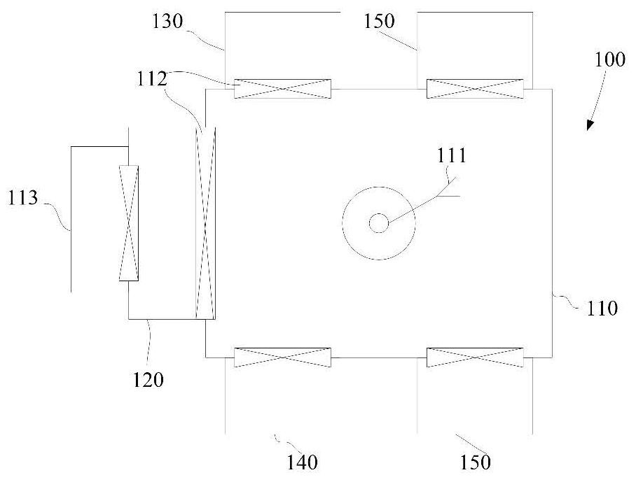
[0067] see figure 1, this embodiment proposes a semiconductor device 100, which may be, for example, a chemical vapor deposition device, or a physical vapor deposition device, or a combination of physical vapor deposition device, chemical vapor deposition device, or other semiconductor devices.

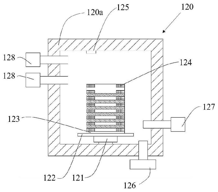
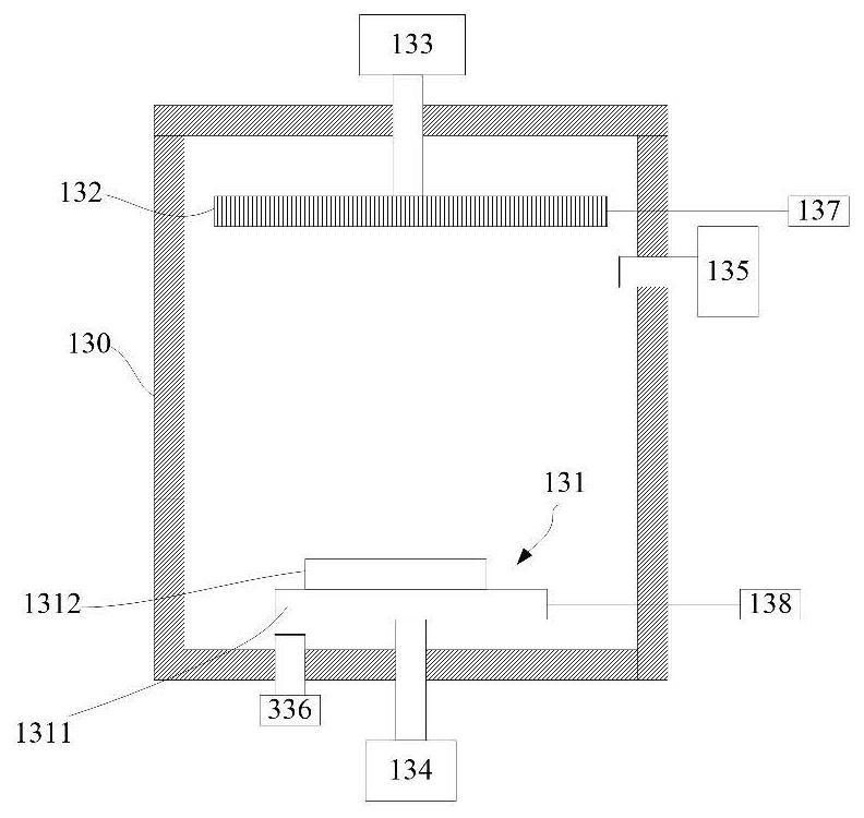
[0068] Such as figure 1 As shown, in one embodiment of the present invention, a plurality of chambers are provided in the semiconductor dev...


PUM

PropertyMeasurementUnit
diameteraaaaaaaaaa
surface areaaaaaaaaaaa
thicknessaaaaaaaaaa

Abstract

The invention provides a semiconductor device, which comprises a preheating cavity. The preheating cavity comprises a shell, a heater arranged at the bottom of the shell and used for placing a substrate, an electrode arranged at the top of the shell and positioned above the substrate, and a lifting rotating mechanism connected with the electrode. According to the semiconductor device provided by the invention, the steps of thin film deposition can be simplified.

Description

technical field [0001] The invention relates to the field of semiconductors, in particular to a semiconductor device. Background technique [0002] With the continuous advancement of integrated circuit production technology, the integration level of circuit chips has been greatly improved. At present, the number of transistors integrated in a chip has reached an astonishing tens of millions, and the signal integration of such a large number of active components requires more than ten layers of high-density metal interconnection layers for connection. Therefore, as an important process for preparing the above-mentioned metal interconnection layer, vapor deposition technology has been widely used. [0003] Traditional semiconductor equipment only provides single-disk transmission in production, which affects the overall production time in mass production. In the current process flow, the preheating chamber preheats the substrate and then transfers the substrate to the cleani...

Claims


Application Information

Patent Timeline
Patent Type & Authority Applications(China)
IPC IPC(8): H01L21/677H01L21/67H01L33/00
CPCH01L21/67781H01L21/67092H01L33/005
Inventor 陈卫军李方华王坤
Owner 苏州辰华半导体技术有限公司
Why Eureka
Try Eureka