PSD type transmission gate image sensor capable of reducing feed-forward effect and manufacturing method thereof

An image sensor and transmission gate technology, which is applied in the design of analog integrated circuits and the design of image sensor pixel circuits, can solve problems such as lowering the potential under the gate, increasing chip power consumption, and increasing process complexity, so as to improve SNR, improve The effect of full well capacity

Pending Publication Date: 2022-01-04
TIANJIN UNIV
View PDF0 Cites 2 Cited by
  • Summary
  • Abstract
  • Description
  • Claims
  • Application Information

AI Technical Summary

Problems solved by technology

The working temperature and integration time can be adjusted according to the requirements of the index. Therefore, the current research focus is mainly to adjust the barrier height of the photodiode and the transmission gate by changing the potential distribution under the transmission gate and the gate. The existing methods to reduce the feedforward effect The method is to adjust the potential distribution by applying negative pressure on the transfer gate (Transfer gate, TG) or changing the doping of the channel under the TG gate. Adding negative pressure can directly pull down the potential under the gate, thereby increasing the PD and TG gate channel. The barrier height of the channel can effectively suppress the feedforward effect, but it also increases the power consumption of the chip, and adjusting the doping under the TG gate increases the complexity of the process

Method used


Image

  • PSD type transmission gate image sensor capable of reducing feed-forward effect and manufacturing method thereof
  • PSD type transmission gate image sensor capable of reducing feed-forward effect and manufacturing method thereof
  • PSD type transmission gate image sensor capable of reducing feed-forward effect and manufacturing method thereof

Examples


Embodiment Construction

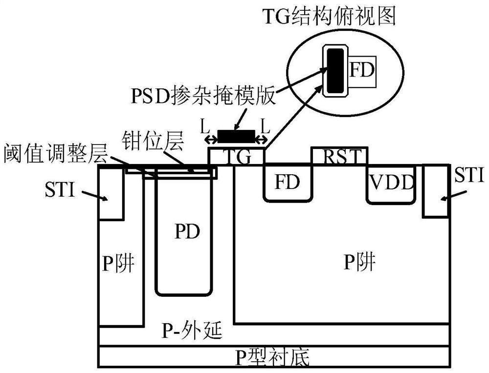
[0015] This solution is mainly through the heavily doped P-type implantation of the transfer gate TG. According to the basic principles of semiconductor physics, the transfer gate channel potential is related to the transfer gate doping. Specifically, it can be analyzed through the following work function:

[0016] When the polysilicon gate is heavily doped with P-type, the Fermi level of the polysilicon gate is close to the top of the valence band, and its work function is greater than that of the P-type substrate:

[0017]

[0018]

[0019] EF pp 、EF pb are the Fermi energy level of P-type doped polysilicon and the Fermi energy level of P-type substrate, N A is the substrate doping concentration. Part of the work function difference between the polysilicon and the substrate falls on the potential difference V between the polysilicon and the substrate surface ms , part of which lands on the space charge region on the substrate surface, so that the potential differenc...


PUM


Abstract

The invention relates to an analog integrated circuit design, and aims to realize large full well and low electric leakage and improve the signal-to-noise ratio and the dynamic range of an image. Therefore, according to the technical scheme adopted by the invention, a PSD type transmission gate image sensor for reducing the feedforward effect comprises a photosensitive region PD, a transmission gate TG for controlling charge transfer from the PD to a storage node FD and a reset tube RST; when light irradiates a semiconductor, a part of light is absorbed by the semiconductor, when the absorbed energy is higher than the width of a silicon forbidden band, and an electron hole pair is generated; under the action of a built-in electric field, photo-induced electrons are collected by a depletion region in the PD; during reading, the TG is turned on, the TG under-gate channel is in a conducting state, photo-generated charges in the PD are transferred into the storage node FD, heavily-doped P-type doping is carried out on the transmission gate TG, low channel closing potential is obtained, and the barrier height of the PD and the channel is increased. The method is mainly applied to the design and manufacturing occasion of the CMOS image sensor.

Description

technical field [0001] The invention relates to the field of analog integrated circuit design, in particular to the field of image sensor pixel circuit design. Background technique [0002] With the rapid development of CMOS image sensors, their applications cover camera, industry, medicine, military and other fields, and people pay more and more attention to the performance of CMOS image sensors. Among them, Signal-to-Noise Ratio (SNR) and Dynamic Range (Dynamic Range, DR) are important parameters to evaluate the imaging performance of the sensor. The signal-to-noise ratio is the ratio of signal to noise, and the maximum signal-to-noise ratio is determined by the full well and the noise. Increasing the full well can improve the signal-to-noise ratio. The dynamic range is the ratio of the maximum signal to the minimum signal detected in the same frame. For a linear sensor, the maximum signal corresponds to the full well capacity of the pixel, while the minimum signal corres...

Claims


Application Information

Patent Timeline
Patent Type & Authority Applications(China)
IPC IPC(8): H01L27/146
CPCH01L27/14614H01L27/14616H01L27/14618H01L27/14636H01L27/14641H01L27/14689
Inventor 徐江涛王倩聂凯明高志远高静
Owner TIANJIN UNIV
Why Eureka
Try Eureka