

Semiconductor heterojunction/homojunction, preparation method thereof and photocatalyst with semiconductor heterojunction/homojunction
A photocatalyst and semiconductor technology, applied in the field of photocatalysis, can solve problems such as low efficiency, achieve the effect of built-in electric field enhancement, flexible energy band structure matching, and improve photocatalytic efficiency
- Summary
- Abstract
- Description
- Claims
- Application Information
AI Technical Summary
Problems solved by technology
Method used
Image

Examples
Embodiment 1
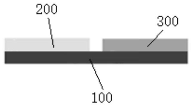
[0064] Semiconductor heterojunction / homojunction: the first semiconductor layer is a 60nm thick CdS film, 0.5nm Pt is used as a co-catalyst, and the second semiconductor layer is 30nm Ag 3 PO 4 thin film, the third semiconductor layer is 30nm Ag 3 PO 4 thin film, the fourth semiconductor layer is a 60nm thick CdS film, the conductive layer is a silver-based alloy with a diameter of 20mm, and the first semiconductor layer and the second semiconductor layer are located on the same side of the conductive layer, and its structure is as follows Figure 6 shown;
[0065] Main raw materials: silver-based alloy (φ20mm), Ag 3 PO 4 Film material (purity 99%), CdS film material (purity 99.999%), Pt film material (purity 99.99%);
[0066] The method of preparing semiconductor heterojunction / homojunction is as follows:
[0067] (1) Silver-based alloy treatment: rinse with distilled water and dry;
[0068] (2) Cover the bow-shaped part of the silver-based alloy that is larger than th...
Embodiment 2
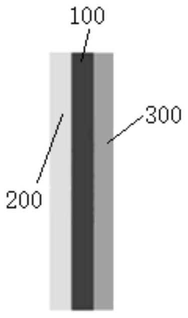
[0094] Its preparation method is the same as that of Example 1, except that the first semiconductor layer and the second semiconductor layer are located on both sides of the semiconductor transition layer, and the obtained semiconductor heterojunction / homojunction is as follows Figure 7 shown.
Embodiment 3
[0096] Its preparation method is the same as embodiment 1, and difference is that the first semiconductor layer is the CdS film of 100nm, and the second semiconductor layer is the thick Ag of 120nm. 3 PO 4 film.
PUM
 Abstract
Description
Claims
Application Information