Preparation method of layer-by-layer self-assembled semiconductor fiber and transistor sensor
A layer-by-layer self-assembly and semiconductor technology, which is applied in fiber processing, plant fiber, ultrasonic/sonic fiber processing, etc., can solve the problems of poor transistor performance, poor cycle stability, and low transconductance, and achieve convenient and excellent detection Effect of selectivity, sensitivity, and low detection limit
- Summary
- Abstract
- Description
- Claims
- Application Information
AI Technical Summary
Problems solved by technology
Method used
Image
Examples
preparation example Construction
[0044] A method for preparing a layer-by-layer self-assembled semiconductor fiber provided by the invention comprises the following steps:
[0045] S1. Prepare an aqueous solution comprising polydiallyldimethylammonium chloride as an electropositive solution, and prepare a mixed solution comprising PEDOT:PSS and multi-walled carbon nanotubes as an electronegative solution;
[0046] The concentration of polydiallyl dimethyl ammonium chloride in the electropositive solution is 0.5~0.75wt%; In the electronegative solution, the concentration of PEDOT:PSS is 1.0~1.3wt%, and the concentration of multi-walled carbon nanotubes is 0.3-0.6wt%. The multi-walled carbon nanotubes are preferably hydroxylated multi-walled carbon nanotubes. The research results of the present invention show that the semiconductor fiber obtained by combining positive and negative electrolytic solutions under this condition is used for the preparation of organic electrochemical transistors and has optimal sens...
Embodiment 1
[0061] A method for preparing a layer-by-layer self-assembled fiber bundle-based organic electrochemical transistor biosensor, comprising the following steps:
[0062] a. Take a section of cotton fiber and carry out surface decontamination treatment, and carry out 1200s of oxygen plasma treatment to obtain a modified fiber bundle;
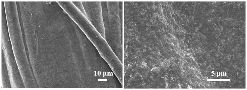
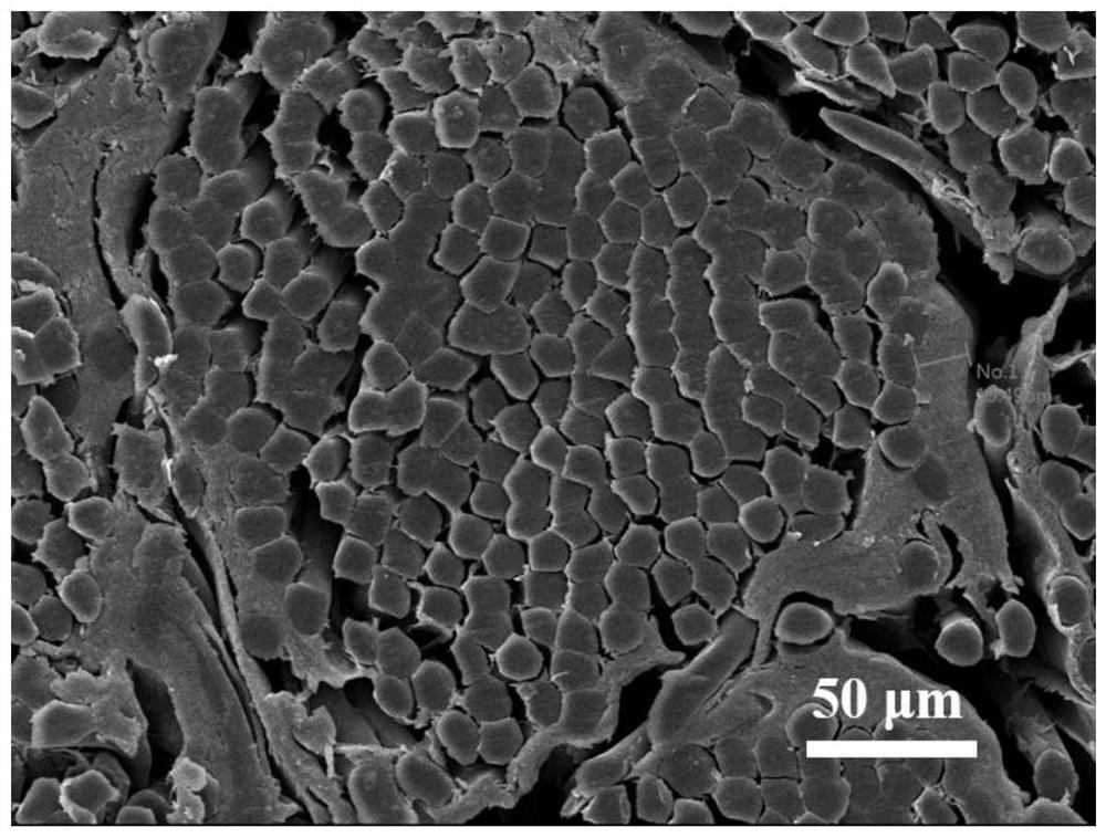
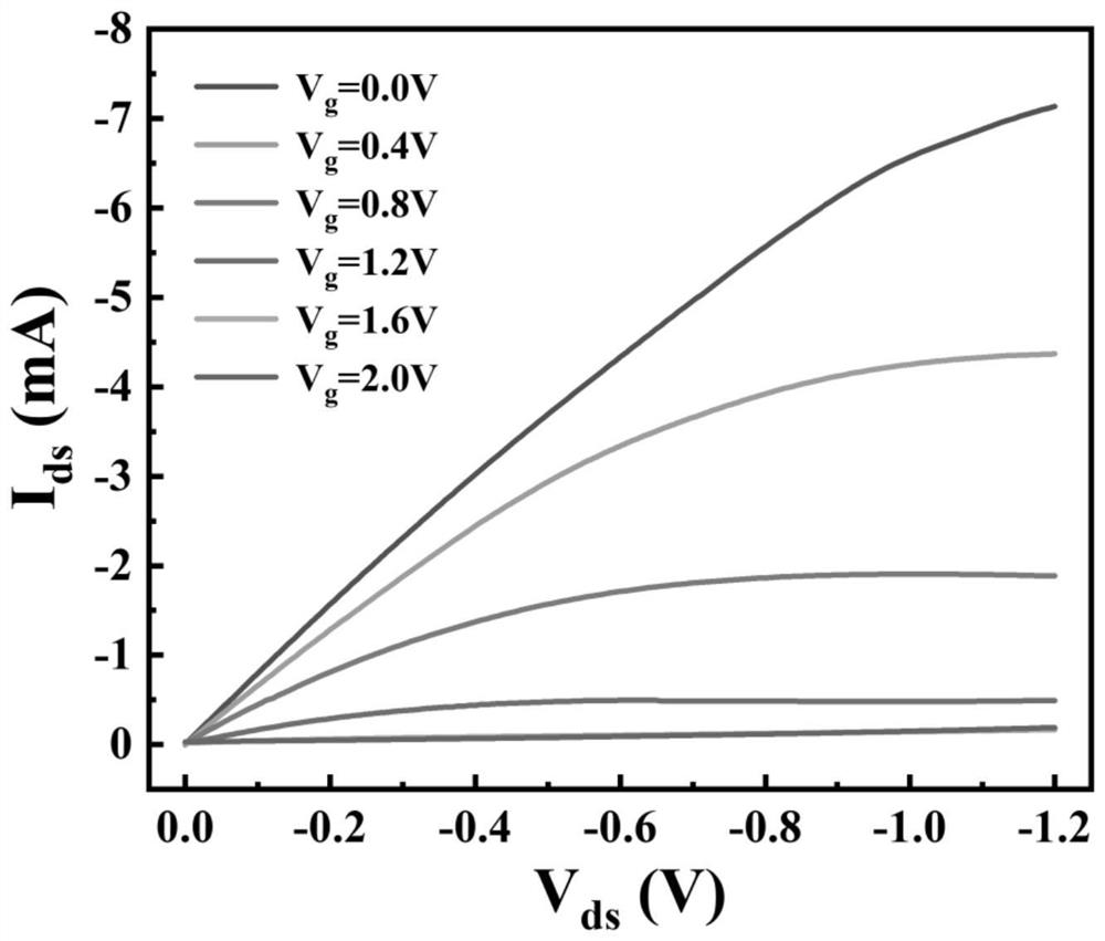
[0063] b. Dissolving the electropositive material PDDA (polydiallyldimethylammonium chloride) in water is prepared into a 0.5wt% electropositive dispersion, PEDOT:PSS (poly(3,4-ethylenedioxy Base thiophene)-poly(styrene sulfonic acid)) concentration is 1wt%, MWCNTs (hydroxylated multi-walled carbon nanotube) concentration is 0.5wt% PEDOT:PSS-MWCNTs composite dispersion liquid as electronegative dispersion liquid, step a The prepared fiber bundles were repeatedly soaked in a certain concentration of electropositive and electronegative dispersions for 10 minutes each, and the composite conductive fiber bundles were obtained by the layer-by-layer self...
Embodiment 2-4
[0083] Compared with Example 1, Examples 2-4 are different in that, in step b, the concentrations of PDDA, PEDOT:PSS, and MWCNTs dispersion are as shown in Table 1, and the others are approximately the same as in Example 1, and are not repeated here. repeat.
[0084] The preparation conditions of table 1 embodiment 2-4
[0085]
[0086] Since PDDA is an electropositive layer and is wrapped by an electronegative layer, its concentration has no significant impact on the performance of fibers and FECT. However, the decrease of the concentration of PEDOT:PSS will reduce the film-forming property, which will affect the conductivity of the composite fiber and the electrochemical performance of FECT. When the concentration of MWCNTs increases, it is more likely to cause the agglomeration of MWCNTs on the surface of the fiber, which affects the conductivity of the composite fiber and the electrochemical performance of FECT.
PUM
 Abstract
Description
Claims
Application Information
 - R&D
- Intellectual Property
- Life Sciences
- Materials
- Tech Scout
- Unparalleled Data Quality
- Higher Quality Content
- 60% Fewer Hallucinations
Browse by: Latest US Patents, China's latest patents, Technical Efficacy Thesaurus, Application Domain, Technology Topic, Popular Technical Reports.
© 2025 PatSnap. All rights reserved.Legal|Privacy policy|Modern Slavery Act Transparency Statement|Sitemap|About US| Contact US: help@patsnap.com


