Optical waveguide chip based on erbium-doped lithium niobate and mode-locked laser
A mode-locked laser, erbium lithium niobate technology, applied in lasers, laser parts, phonon exciters, etc., can solve the problems of high electrical power consumption, high pump light power consumption, large electrode spacing, etc. Modulation of voltage and electrical power consumption, improved pumping efficiency, and low noise effects
Pending Publication Date: 2022-01-07
SHANGHAI JIAO TONG UNIV
View PDF4 Cites 0 Cited by
- Summary
- Abstract
- Description
- Claims
- Application Information
AI Technical Summary
Problems solved by technology
However, the waveguide formed by titanium diffusion is very wide, resulting in a large distance between the electrodes. A very high modulation voltage must be applied to generate a strong enough electric field to achieve effective modulation by changing the refractive index of lithium niobate through the electro-optic effect, and the power consumption is very high.
Titanium diffusion waveguide has poor confinement of signal light and pump light mode spots, resulting in poor overlap between the two, low pump efficiency, and high power consumption of pump light
In addition, the pump light input and the signal light output are on the same side, resulting in the need for an additional wavelength division multiplexer to distinguish between the two, increasing the cost
Method used
View moreImage
Smart ImageViewing Examples
Examples
Embodiment
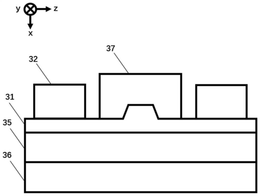
[0058] The thickness of the erbium-doped lithium niobate film is 0.6 microns, the thickness of the silicon dioxide cladding is 2 microns, and the thickness of the silicon substrate is 400 microns. Erbium-doped lithium niobate waveguide etching depth is 300nm. Erbium-doped concentration 1×10 20 cm -3 . The wavelength of pump light is 1480nm. The metal electrode material is gold with a thickness of 600nm. The upper cladding is silica with a thickness of 2 microns.
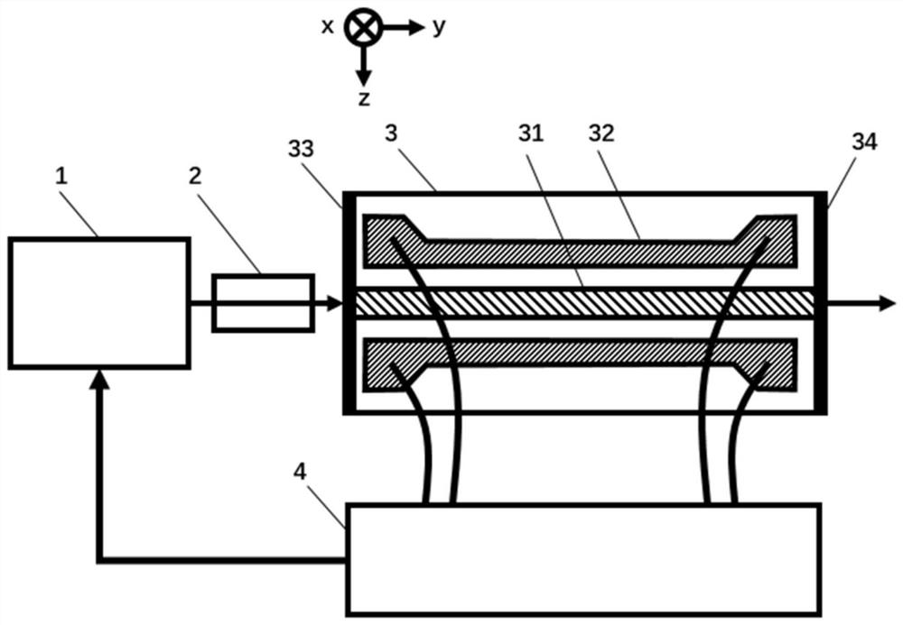
[0059] figure 1 A structural schematic diagram of the present invention is provided, figure 2 A schematic diagram of the chip cross-section is given.
Login to View More PUM
 Abstract
The invention discloses an optical waveguide chip based on erbium-doped lithium niobate and a mode-locked laser. The chip sequentially comprises a substrate, a silicon dioxide cladding, an erbium-doped lithium niobate film and a radio frequency electrode from bottom to top; the erbium-doped lithium niobate thin film is etched through photoetching, and a ridge-type erbium-doped lithium niobate waveguide is formed; and the radio frequency electrodes are arranged on the two sides of the erbium-doped lithium niobate waveguide in parallel. The erbium-doped lithium niobate thin film is used as the waveguide, the low-noise gain characteristic of the erbium-doped waveguide is reserved, the electro-optical characteristic of the lithium niobate waveguide is introduced, the gain and modulation requirements of the active mode-locked laser are met, and the integrated active mode-locked laser which is low in noise and continuously adjustable in repetition frequency can be achieved in cooperation with direct-current bias. The distance between electrodes is reduced through the ridge-type erbium-doped lithium niobate waveguide, the needed modulation voltage and electric power consumption are reduced, overlapping of signal light and pump light speckles can be increased through strong constraint on the signal light and the pump light speckles, and the pump efficiency is improved.
Description
technical field [0001] The invention relates to a mode-locked laser, in particular to an optical waveguide chip and a mode-locked laser based on erbium-doped lithium niobate. Background technique [0002] Integrated mode-locked lasers have important applications in optical signal processing, optical frequency combs and other fields. Traditional integrated mode-locked lasers are mainly based on III-V semiconductor materials, but the lifetime of the upper-level particles of semiconductor materials is only nanoseconds, resulting in a large noise in the mode-locked pulse signal. In high-precision optical signal processing, optical frequency comb It cannot be applied in occasions that require high noise characteristics of the laser. In contrast, the upper-level particle lifetime of erbium-doped waveguides can reach milliseconds, which can provide gain while ensuring low-noise operation of mode-locked lasers. The team of Professor Ippen from the Massachusetts Institute of Techno...
Claims
Login to View More Application Information
Patent Timeline
 IPC IPC(8): H01S3/063H01S3/098
CPCH01S3/1109H01S3/0632H01S3/0637
Inventor 吴侃陈建平
Owner SHANGHAI JIAO TONG UNIV


