
Preparation method for mode field conversion coupling structure and preparation structure of the mode field conversion coupling structure

A technology of coupling structure and mode field conversion, which is applied in the coupling of optical waveguide, light guide, optics, etc., can solve the problems of high structural processing precision, low wavelength sensitivity, and reduced production efficiency, and achieve large processing size and high process efficiency. Simple, avoid high roughness effect

Pending Publication Date: 2022-01-25
嘉兴微智光子科技有限公司
View PDF0 Cites 2 Cited by
  • Summary
  • Abstract
  • Description
  • Claims
  • Application Information

AI Technical Summary

Problems solved by technology

It has the advantages of high coupling efficiency and low wavelength sensitivity. However, due to its small structure size and extremely high requirements for structure processing accuracy, it is often necessary to use a preparation method with a line width that is much smaller than the characteristic size of the photonic chip waveguide. For example, such as Deep / extreme ultraviolet lithography, electron / ion beam direct writing and other methods are used for processing, which will greatly increase the process cost and reduce the production efficiency

Method used


Image

  • Preparation method for mode field conversion coupling structure and preparation structure of the mode field conversion coupling structure
  • Preparation method for mode field conversion coupling structure and preparation structure of the mode field conversion coupling structure
  • Preparation method for mode field conversion coupling structure and preparation structure of the mode field conversion coupling structure

Examples


Embodiment Construction

[0047] In order to better understand the present invention, the present invention will be described in further detail below in conjunction with the examples and accompanying drawings, but the embodiments of the present invention are not limited thereto.

[0048] Taking a lithium niobate on insulator (LNOI) photonic chip as an example, the waveguide on the chip has a width of 1 μm and a thickness of 500 nm. A 100 μm thick polyethylene film was used as a cover, exposing only the 300 μm long end of the waveguide. Use golden velvet polishing cloth and silica ball polishing liquid with a particle size of 20nm as the polishing liquid. Polishing at a rotating speed of 50r / min and a polishing time of 4min can realize a tapered waveguide structure with a length of 300μm and a terminal thickness and width close to 0. The relationship between polishing time and the size of the tapered structure is shown in the table below.

[0049] polishing time Conical structure length ...


PUM


Abstract

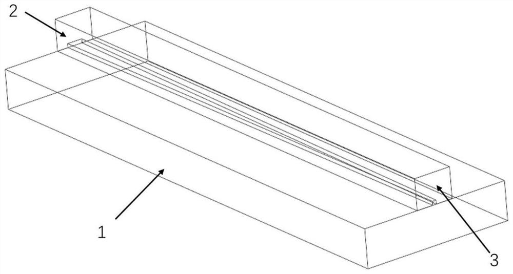
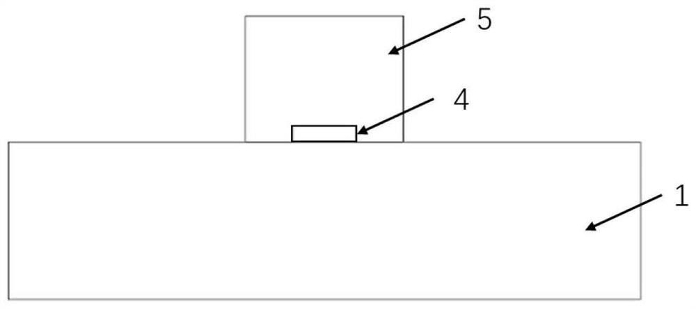
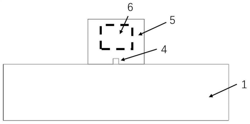
The invention discloses a multilayer coupling structure for photon chip mode field conversion, the lower layer in the coupling structure is a conical structure, the upper layer is an optical waveguide structure with a large size, and a light beam transmitted in the lower layer conical structure is gradually transferred to the upper layer optical waveguide structure for transmission. High-efficiency light beam transmission between the photon chip and the optical fiber is achieved, and the advantages of being low in coupling loss and easy to prepare are achieved. The invention further discloses a structure preparation method based on the chemical mechanical polishing method. The structure preparation method has the advantages of being low in cost, high in machining efficiency, simple in process, high in yield and the like.

Description

technical field [0001] The invention relates to the field of preparation of coupling structures for mode field conversion, in particular to the field of multilayer coupling preparation for mode field conversion of photonic chips. Background technique [0002] Large-scale photonic integrated chips are the key devices to realize future optical quantum technology, high-speed optical communication and optical information processing technology. The cross-sectional size of the optical waveguide on the photonic chip is usually sub-micron, and such a small size provides the possibility for large-scale integration; but on the other hand, since modern optical transmission networks are built on optical fibers, the cross-sectional size of standard communication optical fibers is usually several microns . When the light wave is transmitted between the optical fiber and the optical waveguide of the photonic chip, the difference in the cross-sectional size of the two leads to extremely lo...

Claims


Application Information

Patent Timeline
IPC IPC(8): G02B6/13G02B6/14G02B6/122G02B6/26
CPCG02B6/13G02B6/14G02B6/122G02B6/26G02B6/1228
Inventor 王鹏
Owner 嘉兴微智光子科技有限公司
Learn More