Preparation method of three-dimensional asymmetric metal-medium functional nano array structure

A technology of functional nanometer and array structure, applied in the direction of microstructure technology, microstructure device, manufacturing microstructure device, etc., can solve the problems of small preparation area and high process cost, and achieve good uniformity, multi-parameter adjustable, excellent polarization Effects of dependent properties

Pending Publication Date: 2022-02-08
厦门大学九江研究院
View PDF0 Cites 0 Cited by
  • Summary
  • Abstract
  • Description
  • Claims
  • Application Information

AI Technical Summary

Problems solved by technology

[0005] At present, the main technologies for the preparation of asymmetric nano-array structures include electron beam lithography (EBL), focused ion beam lithography (FIB) and other processing technologies. The process costs are high and the preparation area is small. Therefore, a low-cost, large-area and high-efficiency method is sought. The processing technology for preparing three-dimensional asymmetric functional nanoarray structures is particularly important

Method used


Image

  • Preparation method of three-dimensional asymmetric metal-medium functional nano array structure
  • Preparation method of three-dimensional asymmetric metal-medium functional nano array structure
  • Preparation method of three-dimensional asymmetric metal-medium functional nano array structure

Examples


Embodiment Construction

[0032] The following will clearly and completely describe the technical solutions in the embodiments of the present invention with reference to the accompanying drawings in the embodiments of the present invention. Obviously, the described embodiments are only some, not all, embodiments of the present invention. All other embodiments obtained by persons of ordinary skill in the art based on the embodiments of the present invention belong to the protection scope of the present invention.

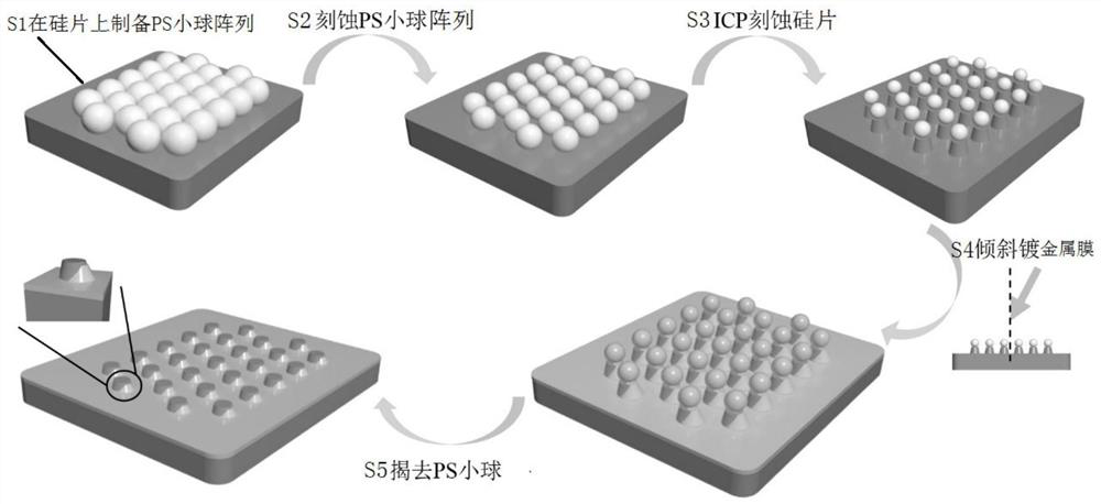
[0033] Such as figure 1 As shown, the method for preparing a three-dimensional asymmetric metal-medium functional nanoarray structure according to an embodiment of the present invention includes the following steps:

[0034] S1 Preparation of polystyrene (PS) bead arrays on sample silicon wafers:

[0035] S11 cleaning the surface of the silicon wafer: immerse the silicon wafer in NH 4 、H 2 o 2 、H 2 In the mixed solution of O, boil at 300°C for 30 minutes, and wash with ultrapure water an...


PUM

PropertyMeasurementUnit
heightaaaaaaaaaa

Abstract

The invention discloses a preparation method of a three-dimensional asymmetric metal-medium functional nano array structure. The preparation method comprises the following steps: S1, preparing a polystyrene sphere array on a sample silicon wafer; S2, etching the polystyrene sphere array; S3, etching the sample silicon wafer; S4, obliquely plating a metal film; and S5, removing polystyrene spheres. The preparation method can solve the problems that a three-dimensional structure is difficult to prepare in a large area and a preparation process is complicated in the existing nano-structure processing field, so that the purposes that large-area preparation is facilitated, prepared products are good in uniformity and adjustable in multiple parameters, a prepared structure has remarkable surface plasmon light amplification and nonlinear enhancement effects, an SHG signal can be enhanced by about five times compared with an SHG signal with a symmetrical structure and has excellent polarization dependence characteristics, the preparation cost is low, and a silicon wafer is adopted as a sample substrate to provide possibilities for application in industrialization of the microelectronic industry in the future are achieved.

Description

technical field [0001] The invention relates to the technical field of micro-nano processing and design of advanced optical functional materials, in particular to a method for preparing a three-dimensional asymmetric metal-medium functional nano-array structure. Background technique [0002] Surface Plasmon Resonance (SPR) can greatly enhance the photoelectric field on the metal surface and localize the light field in the nanometer scale, so SPR has been widely used in new light field regulation, biosensing, Enhanced spectroscopy, nano energy and other fields, and high SPR active nanostructures are the basis for promoting the continuous development of surface plasmon resonance in these fields. [0003] In terms of material selection, different from traditional SPR materials such as gold and silver, aluminum is rich in reserves, low in price, and its working band is not limited by the visible and near-infrared spectral range. It is an important candidate material for the prep...

Claims


Application Information

Patent Timeline
Patent Type & Authority Applications(China)
IPC IPC(8): B81C1/00
CPCB81C1/00031B81C1/00531B81C1/00444
Inventor 沈舒婷高稔现沈少鑫杨志林
Owner 厦门大学九江研究院
Why Eureka
Try Eureka