Submicron single-photon-magnitude tiny light spot measurement method based on silicon photomultiplier tube
A technology of silicon photomultiplier tube and measurement method, which is applied in the field of optical measurement and semiconductor optoelectronics, can solve the problems that pulse spot measurement cannot be realized, and achieve the effect of easy alignment
- Summary
- Abstract
- Description
- Claims
- Application Information
AI Technical Summary
Problems solved by technology
Method used
Image
Examples
Embodiment
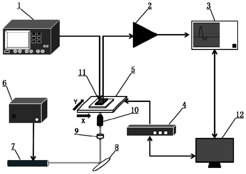
[0065] As shown in Figure 1, the silicon photomultiplier tube 11 models adopted in the present embodiment are respectively selected from FBK (LF-HD, produced in Italy), NDL (EQR1011-1010C-T, produced in China) Hamamatsu S12571-010C (produced in Japan); The nano-shift stage 5 is nanoXYZ (no-load resolution 2nm; displacement range, 200 microns, made in Germany); microscope (including microscope objective lens 10 (model HAS-Y-2-40, bandwidth 10kHz-1.9GHz, noise factor 4.9dB , voltage gain 40dB (100×), made in Germany), pinhole light-transmitting sheet 9, laser beam splitter 8) is X-73, Olympus Corp., (produced by Olympus Corporation in Japan); the picosecond pulse laser is PDL-800D375 (center wavelength, 375nm; full width at half maximum, 44ps; repetition rate, 31.125kHz–80MHz; maximum average light energy, 0.7mW; made in Germany); digital oscilloscope 4 is DPO4102B-L for digital phosphor oscilloscope (sampling rate 5GSa / s, 1GHz bandwidth, produced by Tektronix in the United Sta...
PUM
 Abstract
Description
Claims
Application Information
 - R&D Engineer
- R&D Manager
- IP Professional
- Industry Leading Data Capabilities
- Powerful AI technology
- Patent DNA Extraction
Browse by: Latest US Patents, China's latest patents, Technical Efficacy Thesaurus, Application Domain, Technology Topic, Popular Technical Reports.
© 2024 PatSnap. All rights reserved.Legal|Privacy policy|Modern Slavery Act Transparency Statement|Sitemap|About US| Contact US: help@patsnap.com


