Semiconductor structure and forming method thereof, and semiconductor device and forming method thereof
A semiconductor and conductive structure technology, applied in semiconductor devices, semiconductor/solid-state device manufacturing, electrical components, etc., can solve problems such as poor electrical performance of semiconductor structures
- Summary
- Abstract
- Description
- Claims
- Application Information
AI Technical Summary
Problems solved by technology
Method used
Image

Examples
Embodiment Construction
[0018] It can be seen from the background art that the current semiconductor structure still has the problem of poor electrical performance. Combining with a semiconductor structure, the reasons for the poor electrical performance of the semiconductor structure are analyzed.
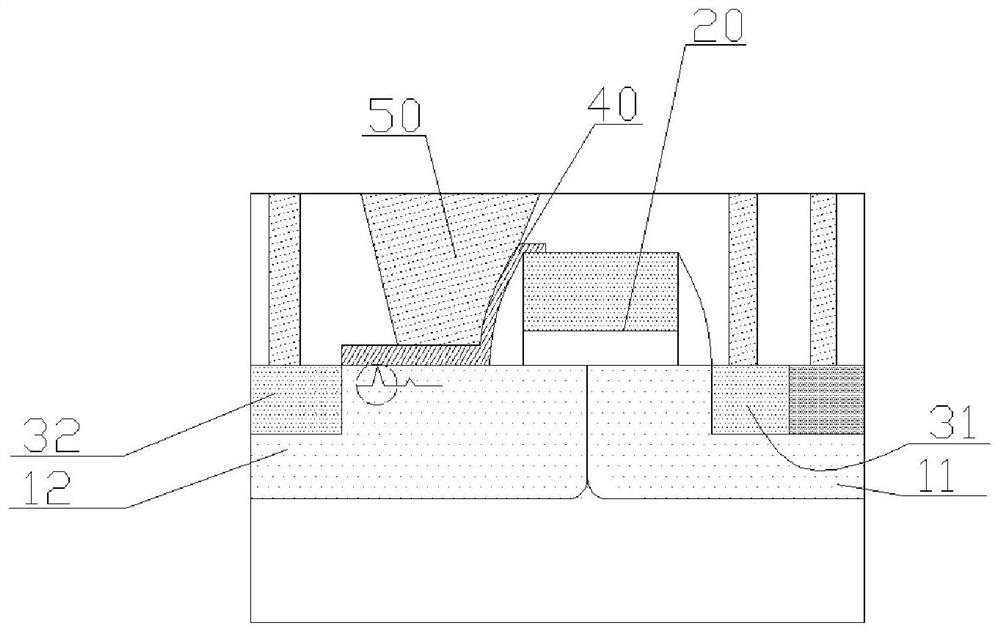
[0019] refer to figure 1 , figure 1 A schematic structural view of a semiconductor structure is shown.
[0020] The semiconductor structure shows a design of an LDMOS, and the semiconductor structure includes: a substrate in which an adjacent well region 11 and a drift region 12 are formed; a gate structure 20 located in the well region 11 Above the substrate at the junction with the drift region 12; the source region 31 is located in the well region 11 on one side of the gate structure 20; the drain region 32 is located in the drift region 12 on the other side of the gate structure 20 . The isolation layer 40 covers part of the top and sidewall of the gate structure 20 and covers the base on the lef...
PUM
 Abstract
Description
Claims
Application Information