Supercharge Your Innovation With Domain-Expert AI Agents!

LED epitaxial structure, preparation method thereof and LED chip

A technology of LED chip and epitaxial structure, which is applied in the direction of electrical components, circuits, semiconductor devices, etc., can solve the problems of reducing the internal quantum efficiency of LED chips and low crystal quality, so as to improve internal quantum efficiency, reduce defect density, and improve crystal growth. quality effect

Pending Publication Date: 2022-03-01
江西乾照光电有限公司
View PDF0 Cites 0 Cited by
  • Summary
  • Abstract
  • Description
  • Claims
  • Application Information

AI Technical Summary

Problems solved by technology

Although a buffer layer is inserted between the substrate and the light-emitting epitaxy, there is still the problem of low crystal quality during epitaxial growth, which reduces the internal quantum efficiency of the LED chip

Method used


Image

  • LED epitaxial structure, preparation method thereof and LED chip
  • LED epitaxial structure, preparation method thereof and LED chip
  • LED epitaxial structure, preparation method thereof and LED chip

Examples


preparation example Construction

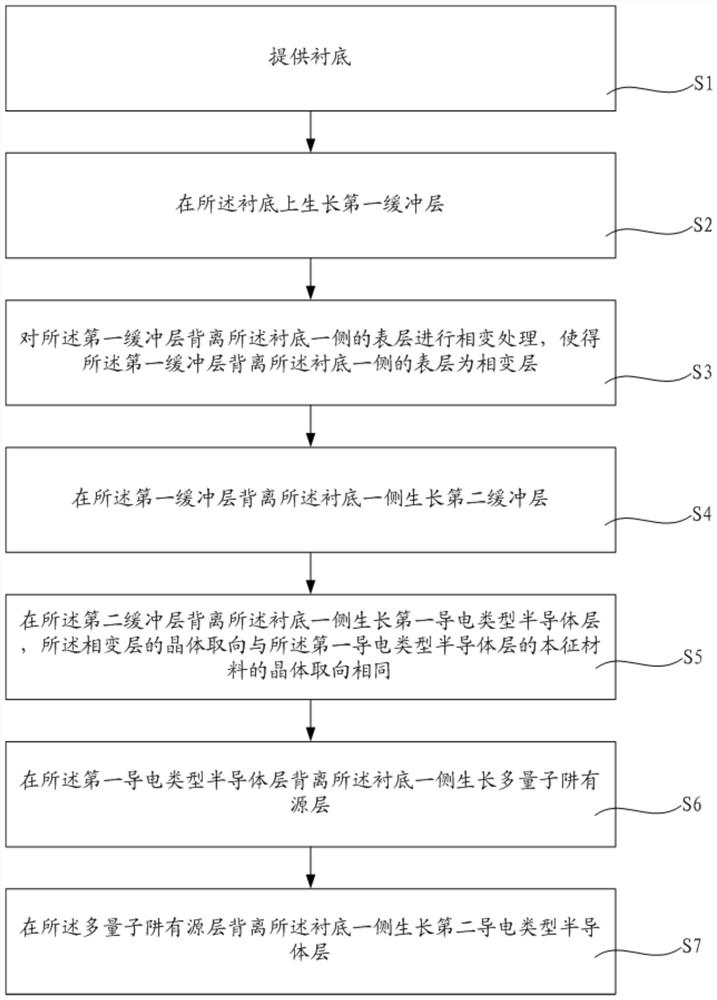
[0044] refer to figure 1 As shown, it is a flow chart of a method for preparing an LED epitaxial structure provided by an embodiment of the present invention, wherein the method for preparing an LED epitaxial structure includes:

[0045] S1. Providing a substrate.

[0046] S2. Growing a first buffer layer on the substrate.

[0047] S3. Perform phase change treatment on the surface layer of the first buffer layer facing away from the substrate, so that the surface layer of the first buffer layer facing away from the substrate is a phase change layer.

[0048] S4. Growing a second buffer layer on a side of the first buffer layer facing away from the substrate.

[0049] S5. Growing a first conductivity type semiconductor layer on a side of the second buffer layer away from the substrate, the crystal orientation of the phase change layer is the same as the crystal orientation of the intrinsic material of the first conductivity type semiconductor layer.

[0050] S6. Growing a mult...


PUM

PropertyMeasurementUnit
Thicknessaaaaaaaaaa
Thicknessaaaaaaaaaa

Abstract

The invention provides an LED epitaxial structure, a preparation method thereof and an LED chip, stress is released through a first buffer layer, and meanwhile transverse growth can be promoted by reducing interface free energy between a substrate and a first conductive type semiconductor layer in the light-emitting epitaxial growth process through a phase change layer; meanwhile, the defect density can be reduced through the growth of the second buffer layer, and finally the crystal growth quality of the LED epitaxial structure is improved, so that the internal quantum efficiency of an LED chip can be improved, and the electric leakage condition of the LED epitaxial structure is improved.

Description

technical field [0001] The present invention relates to the technical field of semiconductors, and more specifically relates to an LED (light-emitting diode, light-emitting diode) epitaxial structure, a preparation method thereof, and an LED chip. Background technique [0002] As a new type of semiconductor solid-state light source, light-emitting diodes have set off a new wave in the field of lighting due to their superior performance, especially GaN-based blue LEDs, which have become a hot spot in international scientific research. With the advancement of science and technology and the improvement of technology level, GaN-based LEDs have made great breakthroughs in luminous efficiency and growth technology, but there are still some problems that need to be solved urgently. Due to the large lattice mismatch and thermal expansion coefficient mismatch between the sapphire substrate and the GaN material, there are some inherent defects in the commercial blue LED based on the s...

Claims


Application Information

Patent Timeline
IPC IPC(8): H01L33/00H01L33/06H01L33/12H01L33/32
CPCH01L33/0066H01L33/06H01L33/12H01L33/325
Inventor 崔晓慧谢祥彬霍丽艳刘兆
Owner 江西乾照光电有限公司
Features
  • R&D
  • Intellectual Property
  • Life Sciences
  • Materials
  • Tech Scout
  • Unparalleled Data Quality
  • Higher Quality Content
  • 60% Fewer Hallucinations
Learn More