Ferroelectric-semiconductor quantum dot coupling enhanced solar cell and preparation method thereof
A technology of solar cells and quantum dots, applied in the field of solar cells, can solve problems such as difficult photoelectric conversion efficiency, and achieve the effects of improving photoelectric conversion efficiency, improving photoelectric conversion efficiency, effective separation and transmission
- Summary
- Abstract
- Description
- Claims
- Application Information
AI Technical Summary
Problems solved by technology
Method used
Image
Examples
preparation example Construction
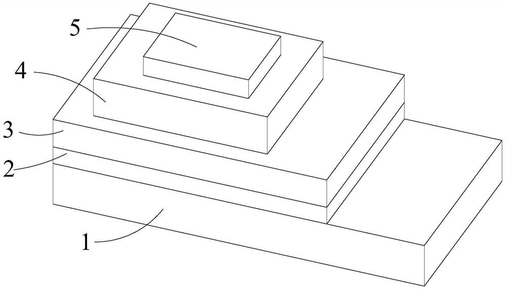
[0069] Based on the same inventive concept, the embodiment of the present application also provides a method for preparing a ferroelectric-semiconductor quantum dot coupling enhanced solar cell, including the following steps:
[0070] S1. Provide substrate;
[0071] S2, preparing an n-type window layer on the surface of the substrate;
[0072] S3. Prepare a ferroelectric layer on the surface of the n-type window layer away from the substrate;
[0073] S4. Prepare a p-type light absorbing layer on the surface of the ferroelectric layer away from the substrate;
[0074] S5. Prepare a top electrode on the surface of the p-type light absorbing layer away from the substrate.
[0075] In some embodiments, the n-type window layer is prepared on the surface of the substrate by pulsed laser deposition, magnetron sputtering or sol-gel method;
[0076] A ferroelectric layer is prepared on the surface of the n-type window layer by a pulsed laser deposition method, a magnetron sputterin...
Embodiment 1
[0100] The embodiment of the present application provides a ferroelectric-semiconductor quantum dot coupling enhanced solar cell, including:
[0101] Substrate;
[0102] n-type window layer, which is located on the surface of the substrate
[0103] a ferroelectric layer located on the surface of the n-type window layer away from the substrate;
[0104] The p-type light absorbing layer is located on the surface of the ferroelectric layer away from the substrate;
[0105] a top electrode, which is located on the surface of the p-type light absorbing layer away from the substrate;
[0106] Among them, the substrate is an ITO transparent conductive glass substrate, the n-type window layer is ZnO, and the ferroelectric layer material is Bi 0.98 Ca 0.02 Fe 0.95 mn 0.05 o 3 , the p-type light-absorbing layer is EDT-modified PbS quantum dots, and the top electrode is Au.
[0107] The preparation method of the above-mentioned ferroelectric-semiconductor quantum dot coupling enh...
Embodiment 2
[0113] The embodiment of the present application provides a ferroelectric-semiconductor quantum dot coupling enhanced solar cell, including:
[0114] Substrate;
[0115] n-type window layer, which is located on the surface of the substrate
[0116] a ferroelectric layer located on the surface of the n-type window layer away from the substrate;
[0117] The p-type light absorbing layer is located on the surface of the ferroelectric layer away from the substrate;
[0118] a top electrode, which is located on the surface of the p-type light absorbing layer away from the substrate;
[0119] Among them, the substrate is an ITO transparent conductive glass substrate, the n-type window layer is ZnO, and the ferroelectric layer material is Bi 0.98 Ca 0.02 Fe 0.95 mn 0.05 o 3 , the p-type light-absorbing layer is EDT-modified PbS quantum dots, and the top electrode is Au.
[0120] The preparation method of the above-mentioned ferroelectric-semiconductor quantum dot coupling enh...
PUM
| Property | Measurement | Unit |
|---|---|---|
| Thickness | aaaaa | aaaaa |
| Thickness | aaaaa | aaaaa |
| Area | aaaaa | aaaaa |
Abstract
Description
Claims
Application Information


