Shield gate groove type field effect transistor of groove type source electrode and preparation method of shield gate groove type field effect transistor
A field effect transistor and shielded gate technology, which is applied in the field of shielded gate trench type field effect transistor and its preparation, can solve the problems of limiting the avalanche capability of the device, increasing the cost of the device, and consuming the area of the silicon wafer, so as to improve the avalanche capability and save energy. Device cost, the effect of reducing silicon area
- Summary
- Abstract
- Description
- Claims
- Application Information
AI Technical Summary
Problems solved by technology
Method used
Image

Examples
Embodiment 1
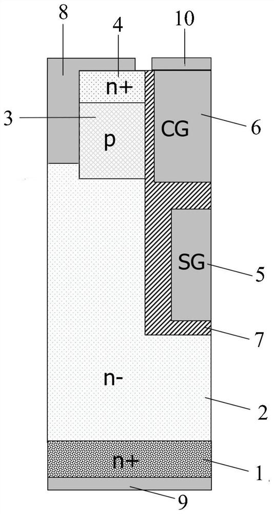
[0048] Both the P-type source region and the N-type source region in the traditional structure are made on the surface of the silicon wafer in the transistor. There are two problems in this structure:
[0049]One is that the structure consumes a certain area of silicon wafers. In order to ensure that the P-type source region has enough area for short-circuiting, the area of the N-type source region must be sacrificed; or in order to ensure that the P-type source region and the N-type source region The area of the area is large, resulting in a large area of silicon wafers and a corresponding increase in device cost; secondly, under this structure, when the transistor is in the forward high voltage blocking or forward high voltage conduction, holes are generated due to the avalanche effect, and the holes The holes will flow through the channel in the base region to form a hole current sufficient to turn on the parasitic triode, triggering the triode to turn on.
[0050] ...
Embodiment 2
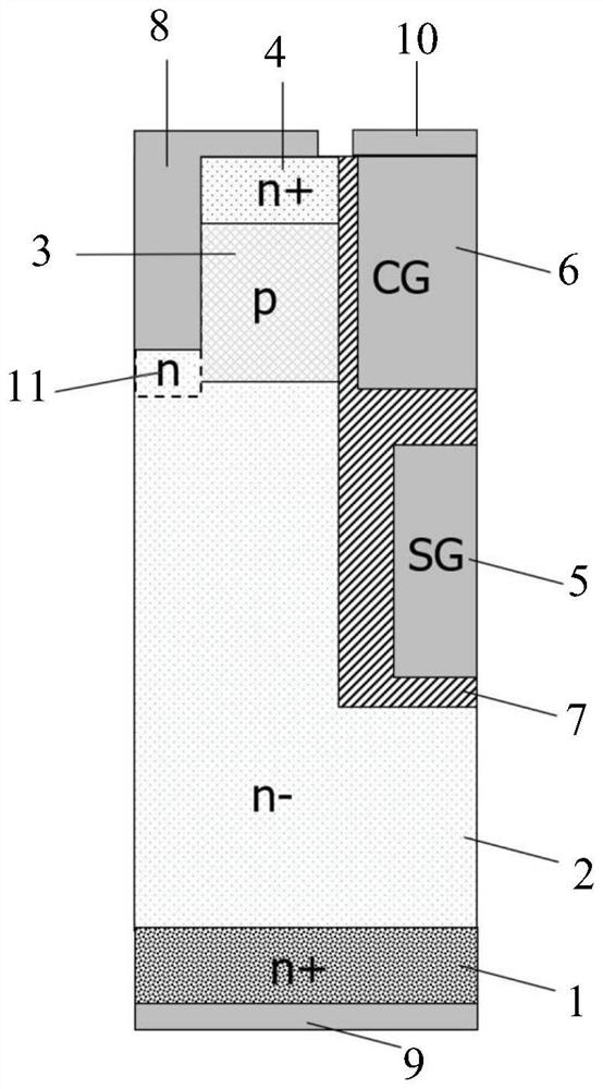
[0068] Based on the shielded gate trench field effect transistor with a trenched source shown in the first embodiment above, the embodiment of the present application provides another structure of a shielded gate trenched field effect transistor with a trenched source, which can be compared with Impurity compensation is performed in the body region to improve the avalanche capability of the transistor.
[0069] The technical solutions of the embodiments of the present application are described in detail below with reference to the accompanying drawings.
[0070] figure 2 It is another structural schematic diagram of a shielded gate trench field effect transistor with a trench source shown in the embodiment of the present application.
[0071] see figure 2 , the shielded gate trench field effect transistor of the trench source, comprising:
[0072] Substrate region 1, drift region 2, base region 3, N-type source region 4, shield gate 5, control gate 6, insulating layer 7, ...
Embodiment 3
[0082] Corresponding to the shielded gate trench field effect transistor with grooved source described in the first embodiment, the present application also provides a method for manufacturing a shielded gate trenched field effect transistor with grooved source and the corresponding Example.
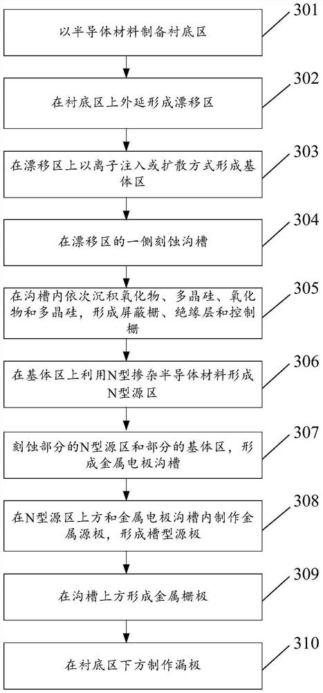
[0083] image 3 It is a schematic flowchart of a method for manufacturing a trench-type source shielded-gate trench field-effect transistor shown in an embodiment of the present application.
[0084] see image 3 , the preparation method of the shielded gate trench field effect transistor of the trench source, comprising:
[0085] 301. Prepare a substrate region with a semiconductor material;
[0086] In the embodiment of the present application, the semiconductor material used is an N-type heavily doped semiconductor material.
[0087] 302. Epitaxially forming a drift region on the substrate region;
[0088] In the embodiment of the present application, different epitaxial processes ...
PUM
| Property | Measurement | Unit |
|---|---|---|
| Width | aaaaa | aaaaa |
Abstract
Description
Claims
Application Information
 - R&D
- Intellectual Property
- Life Sciences
- Materials
- Tech Scout
- Unparalleled Data Quality
- Higher Quality Content
- 60% Fewer Hallucinations
Browse by: Latest US Patents, China's latest patents, Technical Efficacy Thesaurus, Application Domain, Technology Topic, Popular Technical Reports.
© 2025 PatSnap. All rights reserved.Legal|Privacy policy|Modern Slavery Act Transparency Statement|Sitemap|About US| Contact US: help@patsnap.com