IGBT (Insulated Gate Bipolar Translator) welding process method

A welding process and solder paste technology, applied in the field of IGBT welding process, can solve the problems of difficult mold removal, affecting product appearance, cavity deterioration, etc., to eliminate missing dents and agglomerations, reduce product appearance failure, reduce tin beads and tin bridge effect

Pending Publication Date: 2022-03-18
YANTAI TAIXIN ELECTRONICS TECH CO LTD
View PDF11 Cites 5 Cited by
  • Summary
  • Abstract
  • Description
  • Claims
  • Application Information

AI Technical Summary

Problems solved by technology

When the solder paste with the same melting point is used for the second soldering, it is easy to cause the voids on the soldered first reflow surface to deteriorate, false soldering or even fall off. The traditional soldering process and technology are likely to cause voids to deteriorate after the second soldering, affecting product quality and quality. In actual application, it will cause excessive temperature rise, which will affect the life and reliability of the product. The second welding is between the DBC and the bottom plate. Especially for large-area DBC substrates, the amount of solder paste used is large, and high temperature is used. Solder paste is easy to produce solder beads and solder bridges, and the amount of flux after soldering is also large around the mold, which makes it difficult to remove the mold, which not only affects the appearance of the product, but also affects production efficiency; long-term use of high-temperature solder paste will reduce the quality of the stencil. and the life of the mold, increasing the replacement frequency of the steel mesh and the mold, resulting in waste of resources

Method used


Image

  • IGBT (Insulated Gate Bipolar Translator) welding process method
  • IGBT (Insulated Gate Bipolar Translator) welding process method
  • IGBT (Insulated Gate Bipolar Translator) welding process method

Examples


Embodiment 1

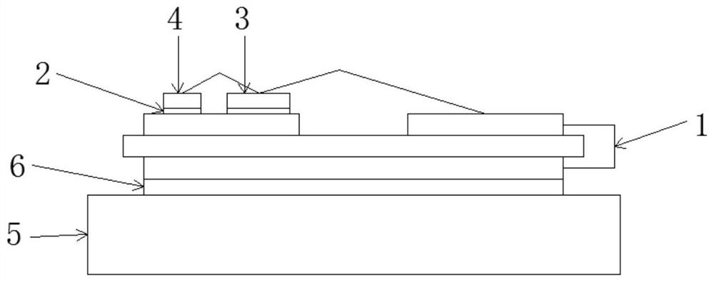
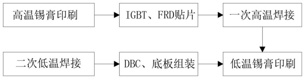
[0032] An IGBT welding process method, IGBT welding materials include DBC ceramic copper clad laminate 1, high temperature solder paste 2, IGBT chip 3, FRD chip 4, metal substrate 5 and low temperature solder paste 6, the specific steps of the welding process include the following steps:

[0033] S1: Print a layer of high-temperature solder paste 2 on the upper surface of the DBC ceramic copper clad laminate 1;

[0034] S2: Place the IGBT chip 3 and the FRD chip 4 on the high-temperature solder paste 2 by an automatic placement machine;

[0035] S3: Load the DBC ceramic copper-clad laminate 1 with the chip attached into the vacuum welding furnace, and perform a high-temperature welding;

[0036] S4: printing a layer of low-temperature solder paste 6 on the upper surface of the metal substrate 5;

[0037] S5: Assemble the DBC ceramic copper-clad laminate 1 after high-temperature welding in step S3 and the metal substrate 5 coated with low-temperature solder paste 6 on the uppe...

Embodiment 2

[0041] An IGBT welding process method, IGBT welding materials include DBC ceramic copper clad laminate 1, high temperature solder paste 2, IGBT chip 3, FRD chip 4, metal substrate 5 and low temperature solder paste 6, the specific steps of the welding process include the following steps:

[0042] S1: Print a layer of high-temperature solder paste 2 on the upper surface of the DBC ceramic copper clad laminate 1;

[0043] S2: Place the IGBT chip 3 and the FRD chip 4 on the high-temperature solder paste 2 by an automatic placement machine;

[0044] S3: Load the DBC ceramic copper-clad laminate 1 with the chip attached into the vacuum welding furnace, and perform a high-temperature welding;

[0045] S4: printing a layer of low-temperature solder paste 6 on the upper surface of the metal substrate 5;

[0046] S5: Assemble the DBC ceramic copper-clad laminate 1 after high-temperature welding in step S3 and the metal substrate 5 coated with low-temperature solder paste 6 on the uppe...

Embodiment 3

[0050] An IGBT welding process method, IGBT welding materials include DBC ceramic copper clad laminate 1, high temperature solder paste 2, IGBT chip 3, FRD chip 4, metal substrate 5 and low temperature solder paste 6, the specific steps of the welding process include the following steps:

[0051] S1: Print a layer of high-temperature solder paste 2 on the upper surface of the DBC ceramic copper clad laminate 1;

[0052] S2: Place the IGBT chip 3 and the FRD chip 4 on the high-temperature solder paste 2 by an automatic placement machine;

[0053] S3: Load the DBC ceramic copper-clad laminate 1 with the chip attached into the vacuum welding furnace, and perform a high-temperature welding;

[0054] S4: printing a layer of low-temperature solder paste 6 on the upper surface of the metal substrate 5;

[0055] S5: Assemble the DBC ceramic copper-clad laminate 1 after high-temperature welding in step S3 and the metal substrate 5 coated with low-temperature solder paste 6 on the upper ...


PUM

PropertyMeasurementUnit
thicknessaaaaaaaaaa
melting pointaaaaaaaaaa

Abstract

The invention discloses an IGBT (Insulated Gate Bipolar Translator) welding process method, which comprises the following steps of high-temperature solder paste printing, IGBT and FRD (Fast Recovery Diode) surface mounting, primary high-temperature welding, copper substrate printing, low-temperature solder paste printing, DBC (Direct Bonding Copper) and bottom plate assembling and secondary low-temperature welding. According to the method, SnPbAg low-temperature solder paste is adopted for secondary welding, after the melting point of the solder paste is reached, secondary melting of soldering tin on a first backflow face is avoided, the phenomenon of deterioration of cavities is avoided, the yield of IGBT products is improved, SnAgCu is adopted as high-temperature solder paste, the melting point of the high-temperature solder paste is 217 DEG C, SnPbAg is adopted as low-temperature solder paste, the melting point of the low-temperature solder paste is 179 DEG C, the melting point is higher than the bearable limit temperature of a chip, the reliability of the products can be guaranteed, and the reliability of the products is improved. The low-temperature solder paste is used for secondary welding, so that tin beads and tin bridges can be reduced, the mold is easy to disassemble, product appearance failure caused by process problems is reduced, the low-temperature solder paste has excellent printability, the phenomena of missing, sinking and caking in the printing process can be eliminated, and the service life of the steel mesh is prolonged.

Description

technical field [0001] The invention relates to the field of welding technology, in particular to an IGBT welding process method. Background technique [0002] The reliability of insulated gate bipolar transistor (IGBT) power semiconductor modules is the focus of attention in production applications. During the packaging process of the IGBT power module, the quality of the solder layer between the chip and the DBC and between the DBC and the metal base plate and the void rate of the solder layer have a direct impact on the working performance and long-term reliability of the IGBT module. [0003] During the IGBT packaging process, two reflow solderings are generally performed. The first soldering is the soldering between the chip and the DBC, and the second soldering is the soldering between the DBC and the metal base. In the prior art, both primary soldering and secondary soldering use SnAgCu solder paste. When the solder paste with the same melting point is used for the ...

Claims


Application Information

Patent Timeline
Patent Type & Authority Applications(China)
IPC IPC(8): B23K1/00B23K1/008
CPCB23K1/0008B23K1/008B23K2101/40
Inventor 姜维宾张茹
Owner YANTAI TAIXIN ELECTRONICS TECH CO LTD
Why Eureka
Try Eureka