Method for controlling thickness of oxide layer on surface of gallium antimonide single crystal

A technology for oxide layer thickness and control methods, applied in chemical instruments and methods, cleaning methods using liquids, cleaning methods and utensils, etc. Problems such as the increase in the thickness of the surface oxide layer, to achieve the effect of controlling the thickness of the oxide layer, meeting the requirements of use, and reducing the contact time

Pending Publication Date: 2022-03-18
INST OF SEMICONDUCTORS - CHINESE ACAD OF SCI
View PDF0 Cites 2 Cited by
  • Summary
  • Abstract
  • Description
  • Claims
  • Application Information

AI Technical Summary

Problems solved by technology

[0003] The traditional surface treatment method of GaSb single crystal material is to use multi-step organic reagents for dewaxing treatment. The steps are cumbersome, the surface is heavily contaminated, and the contact with air is frequent during the treatment process, and the contact time with organic reagents is long, which will cause surface oxidation. The increase of layer thickness causes great differences in the thickness, composition, uniformity and compactness of the oxide layer formed on the surface of GaSb, and the properties of the surface oxide layer will directly affect the deoxidation temperatur

Method used


Image

  • Method for controlling thickness of oxide layer on surface of gallium antimonide single crystal
  • Method for controlling thickness of oxide layer on surface of gallium antimonide single crystal
  • Method for controlling thickness of oxide layer on surface of gallium antimonide single crystal

Examples


example 1

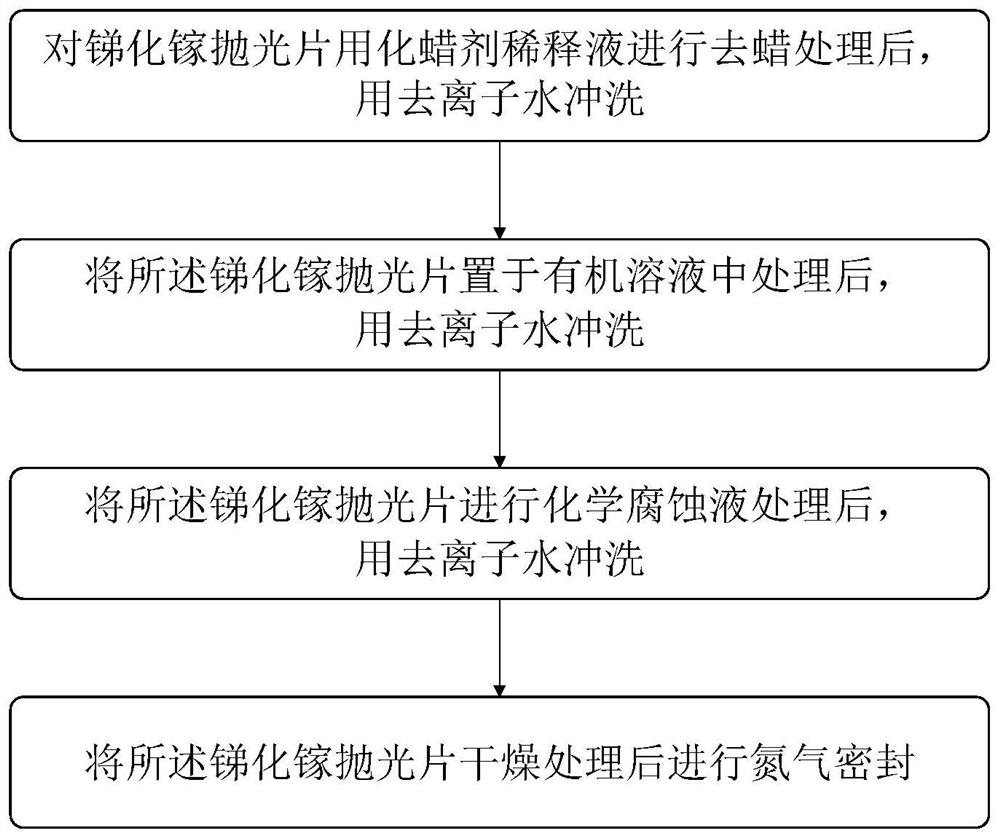
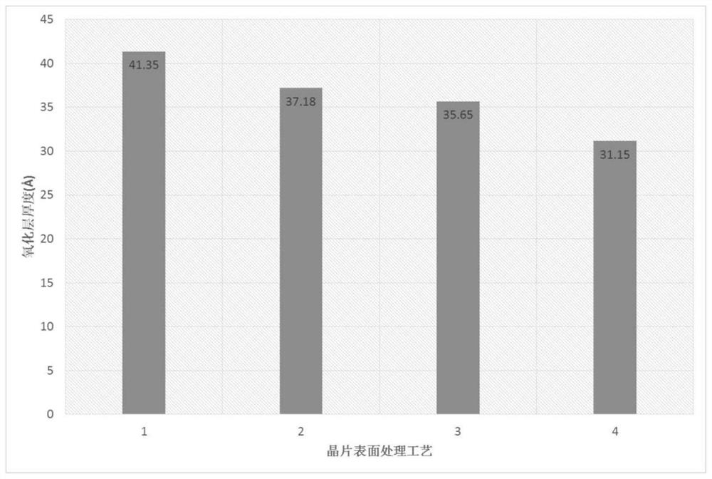
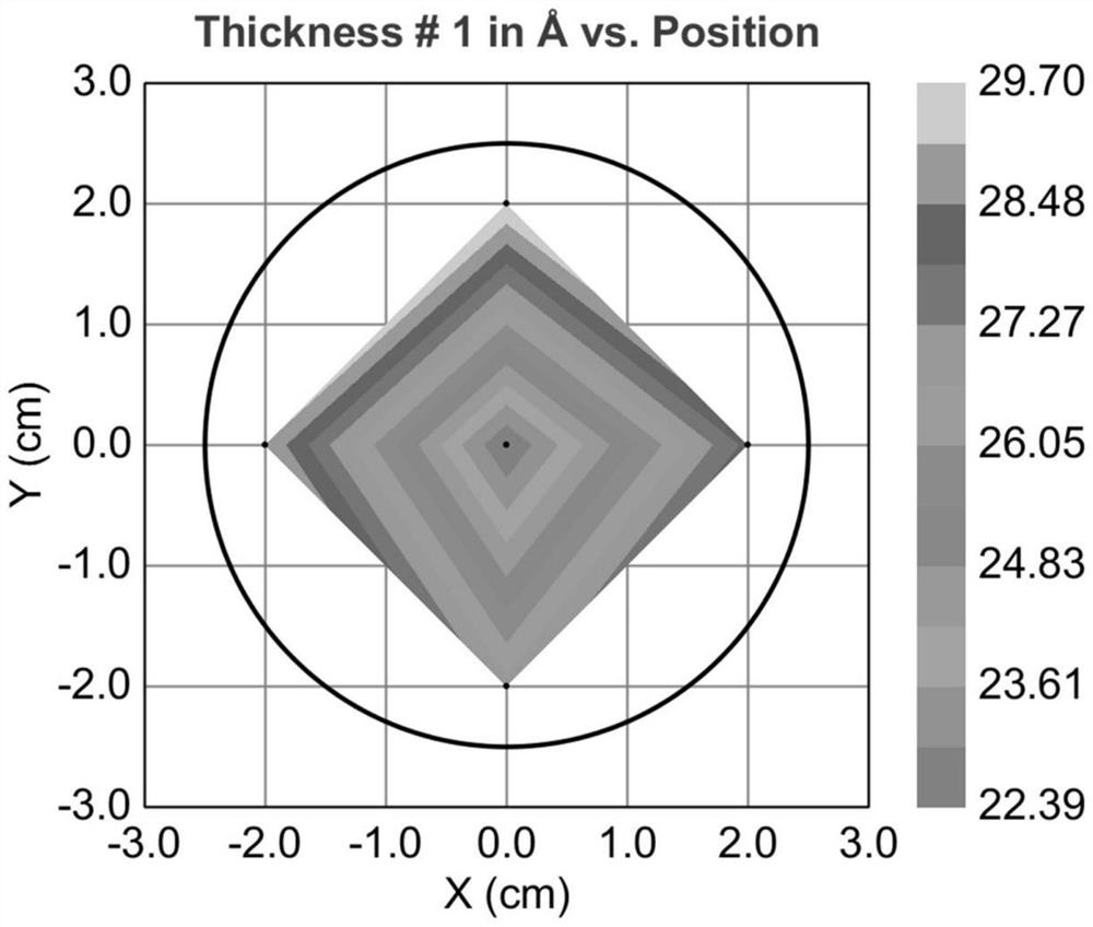
[0035] The method for controlling the thickness of the oxide layer on the surface of the gallium antimonide single crystal includes: treating the gallium antimonide polished piece with a diluent of wax remover, an organic solution and a chemical corrosion solution, specifically, including:

[0036] S1: After immersing the gallium antimonide polished wafer in a diluent of wax remover (40% wax remover) at 85°C for 1 min, take it out and spray and rinse the gallium antimonide wafer surface with deionized water for 40 seconds;

[0037] S2: Place the gallium antimonide polished sheet obtained in S1 in isopropanol solution at 25°C for 30s, and rinse with deionized water for 20s;

[0038] S3: Soak the gallium antimonide polished sheet obtained in S2 in a chemical etching solution at 20°C for 1 minute, and then rinse it with deionized water for 20 seconds, wherein the composition of the chemical etching solution is deionized water with a volume fraction of 78%, Volume fraction is 2% hyd...

example 2

[0055] The method for controlling the thickness of the oxide layer on the surface of the gallium antimonide single crystal includes: treating the polished gallium antimonide sheet with a diluent of wax remover, an organic solution and a chemical corrosion solution, specifically, including:

[0056] S1: After immersing the gallium antimonide polished wafer in 80°C waxing agent diluent (the waxing agent content is 40%) for 1 min, take it out and spray and rinse the gallium antimonide wafer surface with deionized water for 60 seconds;

[0057] S2: Place the gallium antimonide polished sheet obtained in S1 in isopropanol solution at 25°C for 1 min, and rinse with deionized water for 40 s;

[0058] S3: After immersing the gallium antimonide polished sheet obtained in S2 in a chemical etching solution at 20°C for 1 minute, rinse it with deionized water for 40 seconds, wherein the composition of the chemical etching solution is deionized water with a volume fraction of 78%, Volume fr...


PUM


Abstract

The invention discloses a method for controlling the thickness of an oxide layer on the surface of a gallium antimonide single crystal, and the method comprises the steps: carrying out the dewaxing treatment of a gallium antimonide polished wafer through a wax melting agent diluent, and then washing the dewaxed gallium antimonide polished wafer with deionized water; the gallium antimonide polished wafer is placed in an organic solution to be treated and then washed with deionized water; treating the gallium antimonide polished wafer with a chemical corrosive liquid, and then washing the gallium antimonide polished wafer with deionized water; and the gallium antimonide polished wafer is subjected to nitrogen sealing after being dried. The wax melting agent diluent, the organic solution and the chemical corrosive liquid are sequentially used for conducting surface wax melting process treatment on the gallium antimonide polished wafer, adsorption of surface particles can be improved, a natural oxide layer generated on the surface can be removed, the contact time of gallium antimonide single crystals and the external environment is shortened, and therefore the thickness of the oxide layer on the surface of gallium antimonide is effectively controlled, and the surface quality of the gallium antimonide polished wafer is improved. The use requirements of epitaxial materials are met.

Description

technical field [0001] The disclosure relates to the field of semiconductor material surface research, in particular to a method for controlling the thickness of an oxide layer on the surface of a III-V compound semiconductor material gallium antimonide single crystal. Background technique [0002] Gallium antimonide (GaSb) substrate is the key basic material for long-wave infrared detectors and focal plane arrays (FPA) in type II superlattice, and has good application prospects in the field of infrared technology. However, the chemical properties of the surface of GaSb material are active. When the surface is exposed to the air or processed by different processes, an oxide layer that cannot emit light but affects the luminous quality of GaSb material will be formed on the surface of GaSb material. The thickness and properties of the oxide layer will vary. Affects the deoxidation process of the subsequent epitaxial process. Therefore, removing the oxide layer on the surface...

Claims


Application Information

Patent Timeline
IPC IPC(8): H01L21/02B08B3/02B08B3/04B08B3/08
CPCH01L21/02052H01L21/02082B08B3/04B08B3/08B08B3/02
Inventor 谢辉赵有文赵士强沈桂英刘京明王凤华
Owner INST OF SEMICONDUCTORS - CHINESE ACAD OF SCI
Why Eureka
Try Eureka