Silicon carbide power semiconductor device testing method

A technology of power semiconductors and testing methods, which is applied in sorting and other directions, can solve the problems of a large number of gate oxide layer defects and limit commercial development, and achieve the effects of ensuring screening efficiency, improving factory yield, and improving screening accuracy

Active Publication Date: 2022-03-22
ZHUZHOU CRRC TIMES SEMICON CO LTD
View PDF9 Cites 1 Cited by
  • Summary
  • Abstract
  • Description
  • Claims
  • Application Information

AI Technical Summary

Problems solved by technology

[0004] Silicon carbide SBD (Schottky Barrier Diode, Schottky diode) and silicon carbide MOSFET (Metal-Oxide-Semiconductor Field-Effect Transistor, Metal-Oxide-Semiconductor Field-Effect Transistor), among which the silicon carbide MOSFET device is a single-stage device, and the turn-on and turn-off speed is relatively fast. Faster, higher requirements for gate reliability are put forward, and due to the physical characteristics of silicon carbide materials, the number of gate oxide layer defects in the gate structure is large, resulting in the early failure rate of the gate of silicon carbide MOSFET devices compared with silicon MOSFET devices are high, which limits their commercial development

Method used


Image

  • Silicon carbide power semiconductor device testing method
  • Silicon carbide power semiconductor device testing method
  • Silicon carbide power semiconductor device testing method

Examples


Embodiment 2

[0072] For better illustration, the detailed technical scheme of the present invention is as Figure 4 As shown, the details are as follows:

[0073] Step 1, conduct a preliminary test based on a certain number of target devices. The devices used for the preliminary test must meet the following requirements: include devices from different tape-out batches, and the tape-out batches must not be less than 3 batches; Devices from different wafers in the same tape-out batch; the number of devices from the same wafer shall not be less than 10.

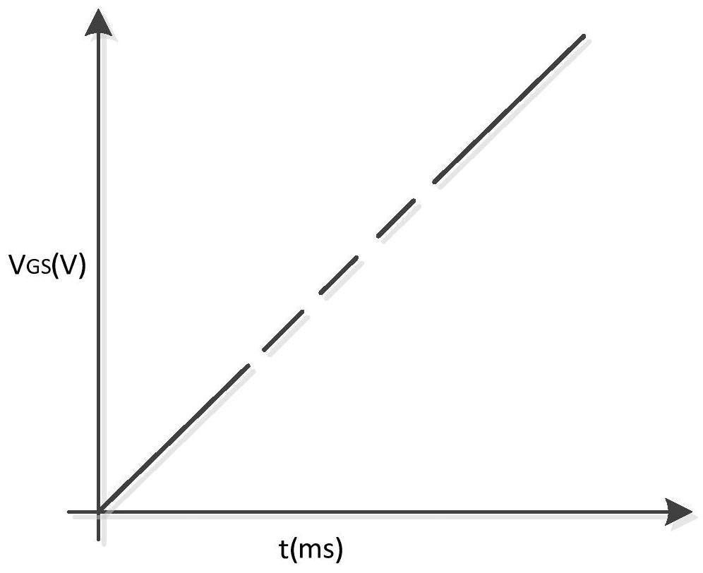
[0074] The bottom-up test is a gate-level leakage test, and the applied gate voltage signal is as follows: figure 2 or image 3 As shown, the test temperature is selected within the maximum allowable operating junction temperature or case temperature of the device. During the test, the gate voltage is continuously increased until the specific gate leakage current is reached, and the gate voltage under the specific gate leakage current is ...


PUM


Abstract

The invention provides a silicon carbide power semiconductor device testing method. The method comprises the following steps: acquiring grid screening reference voltage; testing to obtain a first rated threshold voltage of each silicon carbide power semiconductor device to be tested; the to-be-tested device grid voltage of each to-be-tested silicon carbide power semiconductor device is tested; when the grid voltage of the to-be-tested device is greater than or equal to the grid screening reference voltage, judging preliminary qualification; testing to obtain a preliminarily qualified second rated threshold voltage of each silicon carbide power semiconductor device to be tested; and when the difference amplitude between the first rated threshold voltage and the second rated threshold voltage is greater than a preset change rate threshold, determining that the silicon carbide power semiconductor device is unqualified, otherwise, determining that the silicon carbide power semiconductor device to be detected is qualified. According to the technical scheme, screening is carried out through the grid leakage current test, the threshold voltage test, the grid voltage comparison and the threshold voltage comparison, damaged chips in the grid leakage current test can be effectively screened out, the screening efficiency is ensured, and the screening precision is improved.

Description

technical field [0001] The invention relates to the technical field of semiconductor devices, in particular to a method for testing silicon carbide power semiconductor devices. Background technique [0002] Silicon carbide power semiconductor devices have the characteristics of high withstand voltage, good thermal stability, low switching loss, and high power density, and are widely used in new energy fields such as electric vehicles, wind power generation, and photovoltaic power generation. [0003] Currently commonly used silicon carbide power semiconductor devices mainly include: [0004] Silicon carbide SBD (Schottky Barrier Diode, Schottky diode) and silicon carbide MOSFET (Metal-Oxide-Semiconductor Field-Effect Transistor, Metal-Oxide-Semiconductor Field-Effect Transistor), among which the silicon carbide MOSFET device is a single-stage device, and the turn-on and turn-off speed is relatively fast. Faster, higher requirements for gate reliability are put forward, and ...

Claims


Application Information

Patent Timeline
Patent Type & Authority Applications(China)
IPC IPC(8): B07C5/344
CPCB07C5/344Y02B70/10
Inventor 张文杰李乐乐宋瓘刘启军陈喜明王亚飞周才能李诚瞻
Owner ZHUZHOU CRRC TIMES SEMICON CO LTD
Why Eureka
Try Eureka